WO2004102196A1 - Apparatus including nanostructures used for separation or analysis, and the preparation and application thereof - Google Patents
Apparatus including nanostructures used for separation or analysis, and the preparation and application thereof Download PDFInfo
- Publication number
- WO2004102196A1 WO2004102196A1 PCT/CN2004/000437 CN2004000437W WO2004102196A1 WO 2004102196 A1 WO2004102196 A1 WO 2004102196A1 CN 2004000437 W CN2004000437 W CN 2004000437W WO 2004102196 A1 WO2004102196 A1 WO 2004102196A1
- Authority
- WO
- WIPO (PCT)
- Prior art keywords
- nanostructure
- active
- nanoparticles
- nanoparticle
- chip
- Prior art date
Links
Classifications
-
- B—PERFORMING OPERATIONS; TRANSPORTING
- B01—PHYSICAL OR CHEMICAL PROCESSES OR APPARATUS IN GENERAL
- B01J—CHEMICAL OR PHYSICAL PROCESSES, e.g. CATALYSIS OR COLLOID CHEMISTRY; THEIR RELEVANT APPARATUS
- B01J20/00—Solid sorbent compositions or filter aid compositions; Sorbents for chromatography; Processes for preparing, regenerating or reactivating thereof
- B01J20/281—Sorbents specially adapted for preparative, analytical or investigative chromatography
- B01J20/286—Phases chemically bonded to a substrate, e.g. to silica or to polymers
-
- B—PERFORMING OPERATIONS; TRANSPORTING
- B01—PHYSICAL OR CHEMICAL PROCESSES OR APPARATUS IN GENERAL
- B01J—CHEMICAL OR PHYSICAL PROCESSES, e.g. CATALYSIS OR COLLOID CHEMISTRY; THEIR RELEVANT APPARATUS
- B01J20/00—Solid sorbent compositions or filter aid compositions; Sorbents for chromatography; Processes for preparing, regenerating or reactivating thereof
- B01J20/28—Solid sorbent compositions or filter aid compositions; Sorbents for chromatography; Processes for preparing, regenerating or reactivating thereof characterised by their form or physical properties
- B01J20/28002—Solid sorbent compositions or filter aid compositions; Sorbents for chromatography; Processes for preparing, regenerating or reactivating thereof characterised by their form or physical properties characterised by their physical properties
- B01J20/28004—Sorbent size or size distribution, e.g. particle size
- B01J20/28007—Sorbent size or size distribution, e.g. particle size with size in the range 1-100 nanometers, e.g. nanosized particles, nanofibers, nanotubes, nanowires or the like
-
- B—PERFORMING OPERATIONS; TRANSPORTING
- B01—PHYSICAL OR CHEMICAL PROCESSES OR APPARATUS IN GENERAL
- B01J—CHEMICAL OR PHYSICAL PROCESSES, e.g. CATALYSIS OR COLLOID CHEMISTRY; THEIR RELEVANT APPARATUS
- B01J20/00—Solid sorbent compositions or filter aid compositions; Sorbents for chromatography; Processes for preparing, regenerating or reactivating thereof
- B01J20/28—Solid sorbent compositions or filter aid compositions; Sorbents for chromatography; Processes for preparing, regenerating or reactivating thereof characterised by their form or physical properties
- B01J20/28002—Solid sorbent compositions or filter aid compositions; Sorbents for chromatography; Processes for preparing, regenerating or reactivating thereof characterised by their form or physical properties characterised by their physical properties
- B01J20/28009—Magnetic properties
-
- B—PERFORMING OPERATIONS; TRANSPORTING
- B01—PHYSICAL OR CHEMICAL PROCESSES OR APPARATUS IN GENERAL
- B01J—CHEMICAL OR PHYSICAL PROCESSES, e.g. CATALYSIS OR COLLOID CHEMISTRY; THEIR RELEVANT APPARATUS
- B01J20/00—Solid sorbent compositions or filter aid compositions; Sorbents for chromatography; Processes for preparing, regenerating or reactivating thereof
- B01J20/28—Solid sorbent compositions or filter aid compositions; Sorbents for chromatography; Processes for preparing, regenerating or reactivating thereof characterised by their form or physical properties
- B01J20/28002—Solid sorbent compositions or filter aid compositions; Sorbents for chromatography; Processes for preparing, regenerating or reactivating thereof characterised by their form or physical properties characterised by their physical properties
- B01J20/28011—Other properties, e.g. density, crush strength
-
- B—PERFORMING OPERATIONS; TRANSPORTING
- B01—PHYSICAL OR CHEMICAL PROCESSES OR APPARATUS IN GENERAL
- B01J—CHEMICAL OR PHYSICAL PROCESSES, e.g. CATALYSIS OR COLLOID CHEMISTRY; THEIR RELEVANT APPARATUS
- B01J20/00—Solid sorbent compositions or filter aid compositions; Sorbents for chromatography; Processes for preparing, regenerating or reactivating thereof
- B01J20/28—Solid sorbent compositions or filter aid compositions; Sorbents for chromatography; Processes for preparing, regenerating or reactivating thereof characterised by their form or physical properties
- B01J20/28014—Solid sorbent compositions or filter aid compositions; Sorbents for chromatography; Processes for preparing, regenerating or reactivating thereof characterised by their form or physical properties characterised by their form
- B01J20/28033—Membrane, sheet, cloth, pad, lamellar or mat
-
- B—PERFORMING OPERATIONS; TRANSPORTING
- B01—PHYSICAL OR CHEMICAL PROCESSES OR APPARATUS IN GENERAL
- B01J—CHEMICAL OR PHYSICAL PROCESSES, e.g. CATALYSIS OR COLLOID CHEMISTRY; THEIR RELEVANT APPARATUS
- B01J20/00—Solid sorbent compositions or filter aid compositions; Sorbents for chromatography; Processes for preparing, regenerating or reactivating thereof
- B01J20/28—Solid sorbent compositions or filter aid compositions; Sorbents for chromatography; Processes for preparing, regenerating or reactivating thereof characterised by their form or physical properties
- B01J20/28014—Solid sorbent compositions or filter aid compositions; Sorbents for chromatography; Processes for preparing, regenerating or reactivating thereof characterised by their form or physical properties characterised by their form
- B01J20/28047—Gels
-
- B—PERFORMING OPERATIONS; TRANSPORTING
- B01—PHYSICAL OR CHEMICAL PROCESSES OR APPARATUS IN GENERAL
- B01J—CHEMICAL OR PHYSICAL PROCESSES, e.g. CATALYSIS OR COLLOID CHEMISTRY; THEIR RELEVANT APPARATUS
- B01J20/00—Solid sorbent compositions or filter aid compositions; Sorbents for chromatography; Processes for preparing, regenerating or reactivating thereof
- B01J20/28—Solid sorbent compositions or filter aid compositions; Sorbents for chromatography; Processes for preparing, regenerating or reactivating thereof characterised by their form or physical properties
- B01J20/28054—Solid sorbent compositions or filter aid compositions; Sorbents for chromatography; Processes for preparing, regenerating or reactivating thereof characterised by their form or physical properties characterised by their surface properties or porosity
- B01J20/28057—Surface area, e.g. B.E.T specific surface area
-
- B—PERFORMING OPERATIONS; TRANSPORTING
- B01—PHYSICAL OR CHEMICAL PROCESSES OR APPARATUS IN GENERAL
- B01J—CHEMICAL OR PHYSICAL PROCESSES, e.g. CATALYSIS OR COLLOID CHEMISTRY; THEIR RELEVANT APPARATUS
- B01J20/00—Solid sorbent compositions or filter aid compositions; Sorbents for chromatography; Processes for preparing, regenerating or reactivating thereof
- B01J20/30—Processes for preparing, regenerating, or reactivating
- B01J20/32—Impregnating or coating ; Solid sorbent compositions obtained from processes involving impregnating or coating
- B01J20/3231—Impregnating or coating ; Solid sorbent compositions obtained from processes involving impregnating or coating characterised by the coating or impregnating layer
- B01J20/3242—Layers with a functional group, e.g. an affinity material, a ligand, a reactant or a complexing group
-
- B—PERFORMING OPERATIONS; TRANSPORTING
- B01—PHYSICAL OR CHEMICAL PROCESSES OR APPARATUS IN GENERAL
- B01J—CHEMICAL OR PHYSICAL PROCESSES, e.g. CATALYSIS OR COLLOID CHEMISTRY; THEIR RELEVANT APPARATUS
- B01J20/00—Solid sorbent compositions or filter aid compositions; Sorbents for chromatography; Processes for preparing, regenerating or reactivating thereof
- B01J20/30—Processes for preparing, regenerating, or reactivating
- B01J20/32—Impregnating or coating ; Solid sorbent compositions obtained from processes involving impregnating or coating
- B01J20/3291—Characterised by the shape of the carrier, the coating or the obtained coated product
- B01J20/3295—Coatings made of particles, nanoparticles, fibers, nanofibers
-
- B—PERFORMING OPERATIONS; TRANSPORTING
- B82—NANOTECHNOLOGY
- B82Y—SPECIFIC USES OR APPLICATIONS OF NANOSTRUCTURES; MEASUREMENT OR ANALYSIS OF NANOSTRUCTURES; MANUFACTURE OR TREATMENT OF NANOSTRUCTURES
- B82Y30/00—Nanotechnology for materials or surface science, e.g. nanocomposites
-
- G—PHYSICS
- G01—MEASURING; TESTING
- G01N—INVESTIGATING OR ANALYSING MATERIALS BY DETERMINING THEIR CHEMICAL OR PHYSICAL PROPERTIES
- G01N33/00—Investigating or analysing materials by specific methods not covered by groups G01N1/00 - G01N31/00
- G01N33/48—Biological material, e.g. blood, urine; Haemocytometers
- G01N33/50—Chemical analysis of biological material, e.g. blood, urine; Testing involving biospecific ligand binding methods; Immunological testing
- G01N33/53—Immunoassay; Biospecific binding assay; Materials therefor
- G01N33/543—Immunoassay; Biospecific binding assay; Materials therefor with an insoluble carrier for immobilising immunochemicals
- G01N33/54313—Immunoassay; Biospecific binding assay; Materials therefor with an insoluble carrier for immobilising immunochemicals the carrier being characterised by its particulate form
- G01N33/54326—Magnetic particles
-
- G—PHYSICS
- G01—MEASURING; TESTING
- G01N—INVESTIGATING OR ANALYSING MATERIALS BY DETERMINING THEIR CHEMICAL OR PHYSICAL PROPERTIES
- G01N33/00—Investigating or analysing materials by specific methods not covered by groups G01N1/00 - G01N31/00
- G01N33/48—Biological material, e.g. blood, urine; Haemocytometers
- G01N33/50—Chemical analysis of biological material, e.g. blood, urine; Testing involving biospecific ligand binding methods; Immunological testing
- G01N33/53—Immunoassay; Biospecific binding assay; Materials therefor
- G01N33/543—Immunoassay; Biospecific binding assay; Materials therefor with an insoluble carrier for immobilising immunochemicals
- G01N33/54313—Immunoassay; Biospecific binding assay; Materials therefor with an insoluble carrier for immobilising immunochemicals the carrier being characterised by its particulate form
- G01N33/54346—Nanoparticles
-
- B—PERFORMING OPERATIONS; TRANSPORTING
- B01—PHYSICAL OR CHEMICAL PROCESSES OR APPARATUS IN GENERAL
- B01J—CHEMICAL OR PHYSICAL PROCESSES, e.g. CATALYSIS OR COLLOID CHEMISTRY; THEIR RELEVANT APPARATUS
- B01J2219/00—Chemical, physical or physico-chemical processes in general; Their relevant apparatus
- B01J2219/00274—Sequential or parallel reactions; Apparatus and devices for combinatorial chemistry or for making arrays; Chemical library technology
- B01J2219/00277—Apparatus
- B01J2219/00497—Features relating to the solid phase supports
- B01J2219/00527—Sheets
-
- B—PERFORMING OPERATIONS; TRANSPORTING
- B01—PHYSICAL OR CHEMICAL PROCESSES OR APPARATUS IN GENERAL
- B01J—CHEMICAL OR PHYSICAL PROCESSES, e.g. CATALYSIS OR COLLOID CHEMISTRY; THEIR RELEVANT APPARATUS
- B01J2219/00—Chemical, physical or physico-chemical processes in general; Their relevant apparatus
- B01J2219/00274—Sequential or parallel reactions; Apparatus and devices for combinatorial chemistry or for making arrays; Chemical library technology
- B01J2219/00583—Features relative to the processes being carried out
- B01J2219/00603—Making arrays on substantially continuous surfaces
- B01J2219/00605—Making arrays on substantially continuous surfaces the compounds being directly bound or immobilised to solid supports
- B01J2219/0061—The surface being organic
-
- B—PERFORMING OPERATIONS; TRANSPORTING
- B01—PHYSICAL OR CHEMICAL PROCESSES OR APPARATUS IN GENERAL
- B01J—CHEMICAL OR PHYSICAL PROCESSES, e.g. CATALYSIS OR COLLOID CHEMISTRY; THEIR RELEVANT APPARATUS
- B01J2219/00—Chemical, physical or physico-chemical processes in general; Their relevant apparatus
- B01J2219/00274—Sequential or parallel reactions; Apparatus and devices for combinatorial chemistry or for making arrays; Chemical library technology
- B01J2219/00583—Features relative to the processes being carried out
- B01J2219/00603—Making arrays on substantially continuous surfaces
- B01J2219/00605—Making arrays on substantially continuous surfaces the compounds being directly bound or immobilised to solid supports
- B01J2219/00612—Making arrays on substantially continuous surfaces the compounds being directly bound or immobilised to solid supports the surface being inorganic
-
- B—PERFORMING OPERATIONS; TRANSPORTING
- B01—PHYSICAL OR CHEMICAL PROCESSES OR APPARATUS IN GENERAL
- B01J—CHEMICAL OR PHYSICAL PROCESSES, e.g. CATALYSIS OR COLLOID CHEMISTRY; THEIR RELEVANT APPARATUS
- B01J2219/00—Chemical, physical or physico-chemical processes in general; Their relevant apparatus
- B01J2219/00274—Sequential or parallel reactions; Apparatus and devices for combinatorial chemistry or for making arrays; Chemical library technology
- B01J2219/00583—Features relative to the processes being carried out
- B01J2219/00603—Making arrays on substantially continuous surfaces
- B01J2219/00605—Making arrays on substantially continuous surfaces the compounds being directly bound or immobilised to solid supports
- B01J2219/00614—Delimitation of the attachment areas
- B01J2219/00621—Delimitation of the attachment areas by physical means, e.g. trenches, raised areas
-
- B—PERFORMING OPERATIONS; TRANSPORTING
- B01—PHYSICAL OR CHEMICAL PROCESSES OR APPARATUS IN GENERAL
- B01J—CHEMICAL OR PHYSICAL PROCESSES, e.g. CATALYSIS OR COLLOID CHEMISTRY; THEIR RELEVANT APPARATUS
- B01J2219/00—Chemical, physical or physico-chemical processes in general; Their relevant apparatus
- B01J2219/00274—Sequential or parallel reactions; Apparatus and devices for combinatorial chemistry or for making arrays; Chemical library technology
- B01J2219/00583—Features relative to the processes being carried out
- B01J2219/00603—Making arrays on substantially continuous surfaces
- B01J2219/00605—Making arrays on substantially continuous surfaces the compounds being directly bound or immobilised to solid supports
- B01J2219/00623—Immobilisation or binding
- B01J2219/00626—Covalent
-
- B—PERFORMING OPERATIONS; TRANSPORTING
- B01—PHYSICAL OR CHEMICAL PROCESSES OR APPARATUS IN GENERAL
- B01J—CHEMICAL OR PHYSICAL PROCESSES, e.g. CATALYSIS OR COLLOID CHEMISTRY; THEIR RELEVANT APPARATUS
- B01J2219/00—Chemical, physical or physico-chemical processes in general; Their relevant apparatus
- B01J2219/00274—Sequential or parallel reactions; Apparatus and devices for combinatorial chemistry or for making arrays; Chemical library technology
- B01J2219/00583—Features relative to the processes being carried out
- B01J2219/00603—Making arrays on substantially continuous surfaces
- B01J2219/00605—Making arrays on substantially continuous surfaces the compounds being directly bound or immobilised to solid supports
- B01J2219/00632—Introduction of reactive groups to the surface
- B01J2219/00637—Introduction of reactive groups to the surface by coating it with another layer
-
- B—PERFORMING OPERATIONS; TRANSPORTING
- B01—PHYSICAL OR CHEMICAL PROCESSES OR APPARATUS IN GENERAL
- B01J—CHEMICAL OR PHYSICAL PROCESSES, e.g. CATALYSIS OR COLLOID CHEMISTRY; THEIR RELEVANT APPARATUS
- B01J2219/00—Chemical, physical or physico-chemical processes in general; Their relevant apparatus
- B01J2219/00274—Sequential or parallel reactions; Apparatus and devices for combinatorial chemistry or for making arrays; Chemical library technology
- B01J2219/00583—Features relative to the processes being carried out
- B01J2219/00603—Making arrays on substantially continuous surfaces
- B01J2219/00639—Making arrays on substantially continuous surfaces the compounds being trapped in or bound to a porous medium
- B01J2219/00641—Making arrays on substantially continuous surfaces the compounds being trapped in or bound to a porous medium the porous medium being continuous, e.g. porous oxide substrates
-
- B—PERFORMING OPERATIONS; TRANSPORTING
- B01—PHYSICAL OR CHEMICAL PROCESSES OR APPARATUS IN GENERAL
- B01J—CHEMICAL OR PHYSICAL PROCESSES, e.g. CATALYSIS OR COLLOID CHEMISTRY; THEIR RELEVANT APPARATUS
- B01J2219/00—Chemical, physical or physico-chemical processes in general; Their relevant apparatus
- B01J2219/00274—Sequential or parallel reactions; Apparatus and devices for combinatorial chemistry or for making arrays; Chemical library technology
- B01J2219/00583—Features relative to the processes being carried out
- B01J2219/00603—Making arrays on substantially continuous surfaces
- B01J2219/00646—Making arrays on substantially continuous surfaces the compounds being bound to beads immobilised on the solid supports
- B01J2219/00648—Making arrays on substantially continuous surfaces the compounds being bound to beads immobilised on the solid supports by the use of solid beads
Definitions
- Device for analysis or separation including nanostructure, preparation method and application thereof
- the present invention relates to a nanostructure carrier for separation or / and analysis, in particular a chip substrate, an enzyme-labeled plate substrate, a planar chromatography strip, and a chromatography gel.
- the invention also relates to a highly sensitive nanostructured active carrier for separation or / and analysis, in particular a chip, a microplate, a flat chromatography reagent strip, and a chromatography gel.
- the invention also relates to a nanostructure-containing labeling system for analysis.
- the invention also relates to a kit, in particular a chip kit, an enzyme labeling kit, and a flat chromatography kit.
- the invention also relates to a method for preparing the above-mentioned related substances and its application, in particular to applications in chip analysis, microplate analysis, planar chromatography strip analysis, and chromatography separation. Background technique
- Carriers especially active carriers with selective reactivity, have been widely used in many aspects, especially in the qualitative and / or quantitative analysis or / and separation of target substances in samples.
- active carriers for separation are affinity chromatography gels.
- Analytical active carriers are, for example, antigens and / or antibody chips.
- the solid phase carriers used are mainly planar carriers (such as substrates for biochips, microplates, etc.) made of inorganic materials, organic materials or composite materials and their derivatives, granular carriers (such as chromatography gels, especially micrometers) Particle chromatography gels) and membrane carriers (such as planar chromatography strips).
- planar carriers such as substrates for biochips, microplates, etc.
- granular carriers such as chromatography gels, especially micrometers) Particle chromatography gels
- membrane carriers such as planar chromatography strips.
- slide derivatives such as amine-based slides, aldehyde-based slides, epoxy-based slides, and polyamino acid-coated slides, etc.
- the immobilized active reagent formed by the immobilization of the active reagent on the substrate is one of the key factors affecting the sensitivity or / and specificity of the biochip detection.
- the immobilization methods mainly include: covalent bond immobilization method, physicochemical adsorption method, embedding method and cross-linking method.
- Physicochemical adsorption methods include specific adsorption methods and non-specific adsorption methods. Examples of non-specific adsorption are ion adsorption. Examples of specific adsorption are affinity adsorption.
- Antigen-antibody reaction, nucleotide pairing reaction, lipophilic reaction, etc. are all affinity adsorption.
- the reaction kinetics conditions of the active reagents need to be optimized, and the sensitivity or / and specificity need to be improved, or / and the reaction time needs to be shortened.
- colloids especially organic particles having a size of 100 nm to 500 nm, are used as a ligand carrier.
- the purpose and effect to be achieved is only to reduce the processing labor of the chip, such as processing steps to process the probe points. Uniform chip.
- US Patent Application No. 20030207296 the focus is on using the nanoparticles themselves as a nucleic acid detection ligand carrier, but the research on nanoparticle-modified substrates is insufficient.
- the current labeling system is mainly a molecular dispersion labeling system, and its sensitivity needs to be improved. Hundreds of laboratories are doing this work. Although some nanoparticles have been introduced into labeling systems to improve detection sensitivity (such as WO 00/72018 A1, US Patent Application No. 20030211488, Chinese Patent Application Nos. 02333538.9, 02137418.X, and 01133527.0, they use colloidal gold as a marker , Plus silver enhancement system), but they are either the labeling substance itself (for example, Chinese patent applications No.
- active carriers such as affinity chromatography stationary phases are also widely used in separation devices such as chromatography devices.
- active carriers such as affinity chromatography stationary phases
- the particles used as the matrix of the chromatographic stationary phase have a larger specific surface area than the substrate, there is still room for improvement in terms of analysis time and chromatographic yield.
- the main purpose of the present invention is to increase the reaction efficiency of the active carrier or / and the label in the analysis and separation at a lower cost, thereby increasing the detection sensitivity or / and specificity, or / and reducing the detection time, or / and providing more Kind of solid-phase support with sufficiently high sensitivity.
- the object of the present invention is achieved through the development of vectors, active vectors and labeling systems. As a result of studies on carriers and active carriers, another object of the present invention is to improve the separation efficiency of the separation medium.
- a nanostructure carrier for separation or / and analysis which comprises a nanostructure region, the nanostructure region comprising a conventional solid-phase carrier and the nanostructures fixed thereon.
- the nanostructure includes non-aligned nanostructure units, and the nanostructure unit includes a protrusion height greater than 3 nm, and at least a one-dimensional dimension at the protrusion half height is 1 to 500 nm, preferably 1 to 100 nm.
- Between nano-convex bodies, and the distribution density of the nano-convex bodies in the nano-structure region is greater than 1 / ⁇ m, preferably greater than 10 / ⁇ m 2 .
- nanoconvex refers to a convex with at least one dimension having a size of 110-1000m, such as a nanoparticle fixed on a solid support or other structure
- nanostructure refers to a structural unit with a size of 1 lOOOnm in at least one dimension, such as a nanoparticle
- nanostructure refers to a structure composed of nanostructured units as a structural unit with a height less than 100Onm, such as a nanostructured unit or a nano Dendrites, deep mounds, nets, or other geometric features formed by the convex bodies, and the interrelationship between the nanostructure units or the nanoconvex bodies (for example, the dendrimers may have an upward or parallel direction to the surface, etc.);
- the dendrimers may have an upward or parallel direction to the surface, etc.
- nanostructure region means that the nanostructure carrier has certain features of the present invention (such as the distribution and distribution of nanostructure units). Density, etc.), which includes the nanostructures and optionally the surface of a conventional solid phase support on which the nanostructures are not immobilized; the term "non-nano The “structural region” refers to a region other than the nanostructured region on the nanostructured carrier. The non-nanostructured region may contain a nanostructure but does not have the characteristics of a nanostructured region.
- the nanostructure carrier of the present invention includes a nanostructure region and optionally a non-nanostructure region.
- the target for separation or / and analysis includes one or more of the following groups of substances: polypeptides, drugs that interact with polypeptides, nucleic acids, and drugs that interact with nucleic acids.
- the nanostructure coverage of the nanostructure region is greater than 20%, preferably greater than 30%.
- a surface area improvement rate of the nanostructure region is more than 200%, preferably more than 300%, and more preferably more than 400%.
- the term "the rate of increase in the surface area of the nanostructure region" refers to the ratio of the specific surface area of the nanostructure region to the conventional solid-phase support contained in it: Specific surface area of the solid support) X 100%.
- the surface area improvement rate can be measured directly or indirectly.
- the adsorption capacity of the nanostructure region is improved by more than 115%, preferably more than 130%, and more preferably more than 150%.
- the selection of the adsorbed substance in the adsorption capacity is performed according to a known method.
- the adsorption amount of the nanostructure region is attenuated
- the rate ratio is less than 90%, preferably less than 80%.
- the term "the adsorption rate decay rate ratio of the nanostructure region” refers to a comparison of the rate of decay of the adsorption amount between the nanostructure region and the conventional solid-phase support contained therein as the target substance decreases in concentration:
- the ratio of the amount of decay rate (the rate at which the adsorption amount in the nanostructure region decays with the decrease of the target concentration / the rate at which the adsorption amount of the conventional solid phase carrier decays with the decrease in the target concentration) X 100%.
- the nanostructure carrier of the present invention has certain nanostructure characteristics (for example, the distribution and distribution density of the nanostructure region and the nanostructure units therein, the coverage ratio of the nanostructure, etc.) and the characteristics of the nanostructure (the surface area improvement rate, the adsorption capacity improvement rate, and the adsorption amount Decay rate ratio, etc.).
- the nanostructure characteristics of the nanostructure carrier of the present invention may be related to the nanostructure mentioned, or may be related to the nanostructure not mentioned.
- the nanostructure carrier of the present invention with certain nanostructure characteristics and nanoproperty characteristics is different from the "nanoparticle-coated carrier". In fact, even conventional carriers are susceptible to nanoparticles, such as processing defects and non-specialized adsorption of fine dust.
- the nanostructure carriers of the present invention are not the nanostructure carriers of the present invention. Even if the carrier is specifically coated with nanoparticles, the obtained nanoparticle-coated carrier does not have the characteristics of the nanostructured carrier of the present invention, especially the characteristics of the nanostructured region, which is not qualitatively different from conventional carriers (for example: surface area The improvement rate, the improvement rate of the adsorption capacity, and the ratio of the decay rate of the adsorption amount, etc.) are not the nanostructure carriers of the present invention.
- the nanostructure carrier of the present invention can be obtained by various methods, but the preparation of the nanostructure carrier of the present invention is a preferred method for preparing the nanostructure carrier of the present invention.
- a preferred nanoparticle concentration is one of the keys to obtaining the nanostructure carrier of the present invention.
- the nanoparticle-coated carrier prepared under conditions other than the preferred concentration does not have the characteristics of the nanostructured carrier of the present invention, and is not the nanostructured carrier of the present invention.
- the nanostructure unit is formed of nanoparticles, and the nanoparticle has a particle size of 1 to 500 nm, preferably 1 to 100 nm, and more preferably 1 to 50 nm.
- the nanoparticle and the solid-phase support, or / and the nanoparticle can be bound by one or more methods, such as: covalent bonding, non-specific physicochemical adsorption, antigen-antibody adsorption, affinity Adsorption, nucleotide pair binding, and thermal binding below softening temperature, etc.
- the binding comprises a solid phase support or / and a linker on the surface of the nanoparticles, the linker comprising surface groups or / and coating organic matter.
- the nanoparticles include inorganic nanoparticles or / and organic nanoparticles and their derivatives, and the inorganic nanoparticles include non-magnetic inorganic nanoparticles and magnetic inorganic nanoparticles,
- the non-magnetic inorganic nanoparticles include non-magnetic metal nanoparticles and non-magnetic non-metallic nanoparticles, and the derivative includes a surface group or / and an organic compound Derivatives.
- the non-metallic nanoparticles include organic nanoparticles of plastic, polysaccharide, latex, and resin particles.
- the inorganic non-magnetic non-metal nanoparticles include oxide nanoparticles including silicon oxide particles, titanium oxide particles, and aluminum oxide particles.
- the non-magnetic metal nanoparticles include gold particles, vanadium particles, and lead particles. Although metal particles such as nanoparticle gold have been used in the rapid detection reagent strip, it is used as a molecular marker substance for particles, rather than as a solid-phase carrier in the method of the present invention.
- the conventional solid-phase carrier includes a solid-state carrier made of one or more of the following groups of materials or a derivative having a size greater than 1000 nm: glass, silicon wafer, silica gel , Ceramics, metal oxides, metals, polymer materials and their composites, the derivatives include derivatives that are combined with surface groups or / and coated organics.
- the solid-phase carrier includes a planar carrier (such as a substrate for a biochip, an enzyme-labeled plate, etc.), a granular carrier (such as a chromatography gel, especially a microparticle chromatography gel), and a membrane carrier (such as a planar chromatography). Article).
- the surface group includes one or more of the following groups: amino, aldehyde, epoxy, aminohydrazine, diethylaminoethyl, diethyl Mono (2-hydroxypropyl) aminoethyl, carboxymethyl, sulfopropyl, mercaptoethylpyridyl, siloxane, thiol, fluorenyl;
- the coated organic matter includes one of the following or A variety of organics: surfactants including polyvinylpyrrolidone, Tween-based surfactants, polyelectrolytes including polyamino acids, lipophilic organics including polysiloxane, including dextran derivatives Substances, agarose derivatives, cellulose derivatives, polyacrylamide and other ion exchange polymers, and affinity substances including heparin sodium, antigens, antibodies.
- the surface group may also be a long-arm derived group R— (CH 2 ) X— , where R is a derived group, and X is equal to or greater than 2, preferably greater than 4, and more preferably greater than 6.
- R is a derived group
- X is equal to or greater than 2, preferably greater than 4, and more preferably greater than 6.
- a nanoparticle derivative such as superhydrophobic silica (CDS7) has an alkyl group, and the surface of the coated derivative has an organic coating group, for example, a polyamino acid has an amino group, and an aminohydrazine-polyamino acid has Amino and aminohydrazino, DEAE-Dextmn have diethylaminoethyl, and the like.
- surfactants such as polyvinylpyrrolidone, polyelectrolytes such as polyamino acids, ion exchange polymers such as DEAE-DextraiK affinity substances such as protein A, etc.
- the coated derivative in the method of the invention may be a single or multiple coated derivative.
- silica particles coated with a dispersant or / and dispersion stabilizer primary coating
- PVP double coating
- protein A triple coating
- the range of organic coatings that can be selected is very large.
- the surface groups or / and coating organics can be immobilized on the nanoparticles or / and conventional solid phase supports.
- the nanostructure carrier includes: a nanoparticle / sheet-based composite, a nanoparticle / micro-particle composite, or a nanoparticle / micro-particle / sheet-based composite. It is emphasized that the nanoparticle / sheet composite, nanoparticle / microparticle composite or nanoparticle / microparticle / sheet composite of the present invention is a nanoparticle / sheet composite as a nanostructure carrier of the present invention , Nanoparticle / microparticle composite or nanoparticle / microparticle / sheet-based composite.
- the nanostructure carrier according to the first aspect of the present invention can be used as an analysis chip nanostructure substrate, an enzyme-labeled plate nanostructure microplate, a planar chromatography nanostructure substrate, a nanostructure separation stationary phase, and a nanostructure chromatography gel. Separation of stationary phases within nanostructures.
- a method for preparing a nanostructured carrier which comprises contacting a suspension of the nanoparticles with the conventional solid-phase carrier and performing an immobilization reaction,
- the weight / volume concentration (g / ml) of the nanoparticles in the suspension during the immobilization reaction is from 5% to 1 / 50,000, or the molar concentration of the nanoparticles is 0.12 to 37.4 nM.
- the determined nanoparticle concentration is one of the key points.
- the nanostructure carrier prepared according to the method of the present invention can be used as an analysis chip substrate, an analysis chip flow path, an enzyme-labeled plate substrate, a planar chromatography reagent strip substrate, and a carrier for chromatography gels.
- the nanoparticle weight / volume concentration (g / ml) is from one-fifth to one-fifteen thousandth, or the nano-particle molar concentration is from 0.12 to 3.74 nM.
- the nanoparticle weight / volume concentration (g / ml) is 1 / 20,000 to 60,000, or the nanoparticle molar concentration is 0.31 to 0.93 nM.
- the method according to the second aspect of the present invention may further include one or more of the following functionalization processes to facilitate binding with other related substances:
- the functionalizing treatment includes introducing the surface group or / and coating an organic substance.
- the method according to the second aspect of the present invention may further include chemically crosslinking the product after the immobilization reaction.
- Crosslinking agents that can be used in the present invention include coupling agents such as epichlorohydrin, urotropine, and the like.
- the method according to the second aspect of the present invention may further include heat treating the product after the immobilization reaction.
- the heat treatment includes heating above 30 ° C, preferably above 37 ° C, more preferably above 40 ° C but below the softening temperature of the solid support and then cooling.
- one of the methods to improve the stability of the nanoparticle-coated substrate is heat treatment at the softening temperature of the solid support.
- the heat treatment at the softening temperature is liable to cause deformation of the solid phase support, which makes application difficult.
- the heat treatment method of the present invention is below the softening temperature, even below several tens of degrees, and on Baidu, it can still produce a sufficiently strong binding between the solid support and the nanoparticles.
- the present invention is not intended to enter the theoretical discussion, but only assumes that the nanoparticles may have thermal properties different from conventional materials.
- the heat treatment method of the present invention does not cause deformation of the solid support.
- a nanostructured active support for a separation or / and analysis reactor which comprises a nanostructured active region, said nanostructured active region comprising a conventional solid-phase support and the An active nanostructure comprising a non-aligned nanostructure unit and an active agent fixed thereon, the nanostructure unit includes a protruding height greater than 3 nm, and at least a one-dimensional dimension protruding at a half height of 1 Nano-convex bodies between 500 nm and 100 nm, and the distribution density of the nano-convex bodies in the nano-structure region is greater than 1 / ⁇ 2 , preferably greater than 10 / ⁇ 2 .
- the term “active region” refers to a region to which the active agent is fixed, and the active region may include the entire solid-phase carrier or only one region of the solid-phase carrier or a plurality of regions independent of each other (such as a microarray chip).
- the term “inactive region” refers to a region other than the active region;
- the term “nanostructured active region” refers to an active region that contains, in addition to the active agent, certain characteristics of the present invention (such as the distribution and distribution of nanostructure units) Density, etc.), including the nanostructures, the active agents fixed on the nanostructures, and optionally the surface of a conventional solid-phase support on which the nanostructures are not fixed (in FIG.
- the nano-structure active area can include the entire solid support or only one or multiple regions of the solid support (such as a nano-structure chip)
- the term "nanostructured chip” includes at least one nanostructured active region (for example, one of a probe microarray) according to the present invention.
- nanostructured active carrier or nanostructured chip of the present invention refers to a region other than the nanostructured active region in the active region.
- the non-nanostructured region may contain nanostructures but does not have nanostructured active regions Characteristics.
- nanoconvex “nanostructured unit”, “nanostructure”, “nanostructured region”, “non-nanostructured region” are defined in the above paragraphs.
- a nanostructured active support includes an active region and optionally a non-active region, and the active region includes a nanostructured active region and optionally a non-nanostructured active region.
- the active agent is an agent that imparts a reactivity (eg, an activity to react with a target) to the nanostructured active carrier, such as an ion exchanger, a drug, a polypeptide, Polysaccharides, vitamins, antibiotics, functional organics, antigens, and viruses, cells or their composition.
- the nanostructured active support of the present invention does not contain a labeling substance (for example, a biochip without fluorescein), and is only used in a reactor. Therefore, the nanostructured active support of the present invention does not include a labeling substance.
- the determined nanostructure characteristics and nanoproperty characteristics make the nanostructure active carrier in the present invention different from the active carrier containing nanoparticles in a general sense.
- the active support in some documents is an active support that includes a solid support and nanoparticles on a solid support, we have surprisingly found in a large number of experiments: different characteristics (such as different Surface morphology) of active carriers, whose activities (such as detection sensitivity) can be very different.
- the nanostructured active carrier of the present invention has certain characteristics before it has certain high activity (such as detection sensitivity).
- the self-assemble metal colloid monolayers of the US patent US6025202 are also fundamentally different from the technical solution of the nanostructure active carrier of the present invention, and the former does not have these characteristics of the nanostructure active carrier of the present invention.
- the active nano-particles attached to the surface of the carrier do not necessarily form the nano-structured active region of the present invention.
- the nanostructure coverage of the nanostructure active region is greater than 30%, preferably greater than 75%.
- the surface area increase rate of the nanostructured active region is more than 200%, preferably more than 400%, and more preferably more than 600%.
- the term "the rate of increase in the surface area of the nanostructured active area” refers to the ratio of the specific surface area of the nanostructured active area to the conventional solid-phase support contained in it: The specific surface area of the conventional solid phase support) X 100%.
- the surface area improvement rate can be measured directly or indirectly.
- the surface area improvement rate of the analysis chip is measured indirectly by coating the entire substrate with active nanoparticles and active reagents, respectively.
- the chip of the present invention has a surface area improvement rate of 8.0 or more.
- the sensitivity improvement rate of the nanostructure active region is greater than 120%, preferably greater than 150%, more preferably greater than 200%, or / and the adsorption capacity improvement rate is greater than 115%, It is preferably more than 130%, more preferably more than 150%.
- the term "non-nano-structured active carrier” refers to an active carrier that does not contain the nano-structured active region of the present invention, such as a chip formed by spotting HCV antigen onto a redox slide (nano-structured activity Examples of carriers are the HCV antigen-coated silicon oxide nano
- the recognition signal decay rate ratio of the nanostructure active region is less than 90%, preferably less than 70%, or / and the adsorption amount decay rate ratio is less than 90%, preferably less than 80 %.
- the term "recognition signal attenuation rate ratio of the nanostructured active region” means that the recognition signal of the nanostructured active region and a non-nanostructured active carrier containing the same conventional solid-phase support and active reagent is lower in the analysis when the target is analyzed.
- Identification signal decay rate ratio (speed at which the identification signal of the nanostructure region decays with the decrease of the target's low concentration / rate at which the identification signal of the non-nanostructure active carrier decays with the decrease of the target's low concentration) X 100%;
- the term "absorption rate ratio of the adsorption amount of the nanostructured active area” refers to the comparison of the rate of decay of the adsorption capacity of the nanostructured area with the non-nanostructured active support containing the same conventional solid-phase support and active reagent as the target concentration decreases.
- Adsorption rate decay rate ratio (the rate at which the adsorption amount of the nanostructured active area decays with the decrease of the target concentration / the rate at which the adsorption amount of the non-nanostructured active support decays with the decrease of the target concentration) X 100%.
- the nanostructure active carrier of the present invention is technically different from the bioactive carrier described in PCT International Patent Application PCT / US96 / 04485 (and CN96193700.9).
- the latter's active nanostructure is a nano whisker aligned by orientation. It is formed, and its preferred manufacturing method is completely different from the preferred manufacturing method of the present invention. As a result, the cost is high and the active nanoparticle array cannot be fixed at a fixed point only on a solid support like a chip of the present invention. .
- the nanostructure active carrier of the present invention is also different from other nanostructure-containing active carriers that have been disclosed.
- the nanostructure active carrier of the present invention has certain nanostructure characteristics (for example, the distribution and distribution density of nanostructure active regions and nanostructure units therein, the coverage ratio of nanostructures, etc.) and the characteristics of nanostructures (surface area increase rate, adsorption capacity increase rate, Adsorption rate decay rate ratio, sensitivity improvement rate, identification signal decay rate ratio, etc.).
- the nano-characteristics of the nano-structured active support of the present invention may be related to the nano-structure mentioned, or may be related to the nano-structure not mentioned.
- the nanostructured active conformation support of the present invention with certain nanostructure characteristics and nanoproperty characteristics is just like the nanostructure support of the present invention with certain nanostructure characteristics and nanoproperty characteristics, which is different from the "nanoparticle-coated carrier" in the ordinary sense. "Same, different from ordinary meaning”
- the nanostructured active carrier of the present invention can be obtained by various methods, but the method of preparing the nanostructured active carrier of the present invention is the preferred method of preparation of the nanostructured active carrier of the present invention. It should be particularly emphasized It is noted that, in the preparation method of the present invention, a preferred active nanoparticle concentration is one of the keys to obtaining the nanostructured active support of the present invention.
- the active nanoparticle is prepared under conditions other than the preferred concentration.
- the nanoparticle-coated active carrier does not have the characteristics of the nanostructured active carrier of the present invention, and is not the nanostructured active carrier of the present invention.
- the active nanoparticle-containing active carrier formed without strict structural design is different from the nanostructure active carrier of the present invention. Only the active carrier having the above characteristics is the nanostructure active carrier of the present invention.
- the nanostructured active carrier of the present invention includes a nanostructured single-active carrier and a nanostructured multi-active carrier, wherein the nanostructured single-active carrier has only one active nanoparticle containing one active agent fixed on the same solid-phase carrier, and The nano-structured multi-active carrier is fixed on the same solid-phase carrier with active nanoparticles containing more than two kinds of active agents.
- the nanostructured single-active carrier has only one active nanoparticle containing one active agent fixed on the same solid-phase carrier
- the nano-structured multi-active carrier is fixed on the same solid-phase carrier with active nanoparticles containing more than two kinds of active agents.
- Devices such as chips and planar chromatography reagent strips
- Carrier means, for example, microtiter plates.
- the target of the separation or / and analysis includes a polypeptide or / and a drug that interacts with the polypeptide.
- active agents that can interact with the target polypeptide, such as ion exchangers, drugs, peptides, polysaccharides, vitamins, antibiotics, functional organics, antigens, and viruses, cells, or their components.
- the active nanostructure and the solid phase carrier may not be bound through nucleotide pairing, for example, in one or more of the following ways: covalent bond binding, non-specific physics Chemisorption, antigen-antibody adsorption, and affinity adsorption, and the binding is achieved by a solid phase support or / and a linker on the surface of the nanoparticle, the linker including surface groups or / and coating organic matter or / And the active agent.
- the binding between the nanoparticle and the substrate must be performed by the pairing of nucleic acids, and it is not suitable for the detection and separation of substances other than nucleic acids such as polypeptides.
- the target for separation or / and analysis includes a nucleic acid or / and a drug that interacts with the nucleic acid.
- the nucleic acid nanoparticle-coated sheet of the present invention Because it has certain nanostructure characteristics and nanoproperty characteristics, it is not the same as the nucleic acid nanoparticle-coated substrate in US Patent Application No. 20030207296.
- the nanostructured active support according to the third aspect of the present invention may be a composite of an active nanoparticle and a solid phase support, wherein the active nanoparticle comprises a nanoparticle and one or more of the active agents or any of the active agents immobilized thereon.
- the particle size of the nanoparticles is 1 to 500 nm, preferably 1 to 100 nm, and more preferably 1 to 50 nm.
- the solid phase support is a conventional solid phase support or the nanometer according to claim 1 to 14. Structure carrier.
- the active nanoparticle / sheet-based composite of the present invention can be obtained by various methods, but the method for preparing the active nanoparticle / sheet-based composite of the present invention is the preferred method of the present invention.
- the nanoparticle includes the nanoparticle according to the first aspect of the present invention, and the preferred solution is the inorganic nonmagnetic nonmetal nanoparticle and the derivative thereof.
- the preferred scheme of the nanostructure active carrier of the present invention includes Nanostructured active support with metal surface and metal nanoparticles.
- the nanostructured active support according to the third aspect of the present invention includes one of the complexes selected from the group consisting of: active nanoparticle / sheet composite, active nanoparticle / microparticle composite, active nanoparticle / nanostructured tablet Composites, active nanoparticle / nanostructured microparticle composites, and combinations thereof.
- the nanostructured active support according to the third aspect of the present invention may be a complex of an active agent and the nanostructured support according to the first aspect of the present invention.
- the nanostructured active support according to the third aspect of the present invention includes one of the complexes selected from the group consisting of: an active agent / nanostructured tablet-based complex, an active agent / nanostructured microparticle complex, and combinations thereof.
- the active nanoparticle / sheet-based composite can be obtained by various methods, but the preparation of the nanoparticle / sheet-based composite of the present invention is the preferred method of the present invention.
- nanostructured active support there is one or more ligands between one or more nanoparticles and the solid support, or / and one or more ligands and the solid support
- One or more nanoparticles, or / and one or more ligands between the at least one heavy nanoparticle and another heavy nanoparticle is prepared, for example, as follows: the carrier is coated with a reassortant 1 to form a ligand 1 coated carrier, and the nanoparticles are prepared.
- Coated with another ligand 2 (pairing reaction can occur between ligands 1 and 2) to form a ligand 2 / nanoparticle complex, and then coat or spot the ligand 2 / nanoparticle complex to the ligand 1 coats the carrier to form a complex in the form of ligand 2-nanoparticles, ligand 2-ligand 1-carrier.
- the number of ligand layers is greater than 2, and so on.
- nanostructured active carriers with multiple ligands between a heavy nanoparticle and another layer of nanoparticles such as ligand 3-nanoparticle-ligand 3-ligand 2-nanoparticle-ligand 2-ligand 1
- a nanostructured active carrier having multiple nanoparticles between one or more ligands and a carrier can be prepared as follows: First, one or more of the nanoparticles are combined with a plurality of the ligands to form multiple activities.
- Nanoparticles (such as Ligand 2—Nanoparticles 1 Ligand 2, Ligand 3—Nanoparticles 1 Ligand 2, Ligand 1—Nanoparticles 1 Ligand 1, etc.), and then these active nanoparticles are bound to On the carrier, for example, ligand 2—nanoparticles—ligand 2—ligand 1—nanoparticles—ligand 1—support, ligand 3—nanoparticles—ligand 2—ligand 1—nacau particle 1— Ligand 1-a nanostructured active carrier in the form of a carrier and the like.
- the nanostructure active carrier according to the third aspect of the present invention can be used as a nanostructure analysis chip.
- it can also be used as a nanostructure enzyme plate, a nanostructure planar chromatography reagent strip, and a nanostructure active separation stationary phase including a nanostructure chromatography active gel.
- a fourth aspect of the present invention provides a method for preparing a nanostructured active support according to the second aspect of the present invention, which comprises contacting a suspension of the active nanoparticle with the conventional solid-phase support and immobilizing the same.
- the reaction and: the weight / volume concentration (g / ml) of the nanoparticles in the suspension during the immobilization reaction is from 5% to 1 / 50,000, or the molar concentration of the nanoparticles is from 0.12 to 37.4 nM;
- the contact is a point contact with a surface diameter of less than 0.5 mm or a surface contact with a surface diameter of more than 0.5 mm.
- An example of the formation of the composite of the active nanoparticle and the solid phase carrier of the present invention is: after the nanoparticle suspension is mixed with the ligand solution to form an active nanoparticle, the mixed solution is spotted on the chip substrate and combined by spotting Reaction, etc.
- the carrier according to the present invention may also be prepared in such a manner as to coexist with other structures, such as a substrate in a multi-chip substrate or the like.
- the active nanoparticles may be nanoparticles and ligands prepared as a mixture with other substances, such as a nanoparticle suspension containing a colorant or / and a binder, a ligand solution containing a stabilizer, and the like.
- the active nanoparticle suspension includes a mixture (such as an unpurified substance after the nanoparticle and the ligand are mixed and reacted) and a purified substance (such as the nanoparticle and the ligand are subjected to centrifugation to remove the purified substance with free ligand), and One or more kinds of ligands are immobilized on a nanoparticle in the purified product. It needs to be particularly emphasized that when the nanoparticles are not sufficiently diluted or over-diluted, no increase in sensitivity is observed for the composites prepared using certain nanoparticles.
- the weight / volume concentration of the nanoparticles (g / ml) It is 1/5000 to 150,000 /, or the molar concentration of nanoparticles is 0.12 to 3.74 nM.
- the weight / volume concentration (g / ml) of the nanoparticles is between 1 / 20,000 and 60,000, or the molar concentration of the nanoparticles is between 0.31 and 0.93 nM.
- the method according to the fourth aspect of the present invention further includes performing a chemical crosslinking treatment on the product after the immobilization reaction.
- the method may further include heat-treating the product after the immobilization reaction, and the heat-treating includes protection above 30 ° C, preferably 37, under the protection of an optional active agent protecting agent. Above C but below the softening temperature of the solid support, it is warmed and then cooled.
- the active agent protective agent includes one or more of the following protective agents: amino acids, proteins, and sugars.
- an analysis or / and separation device comprising a nanostructured support according to the first aspect of the invention or / and a nanostructured active support according to the third aspect of the invention. It includes devices for polypeptide analysis, nucleic acid analysis, or / and pharmaceutical analysis.
- the nanostructured active carrier according to the present invention can be used as an analysis chip, an enzyme plate, a flat chromatography reagent strip, and a chromatography gel, or a component device thereof.
- the device includes one of the following analysis chips: a microarray chip, a microarray chip, and a flow path chip, wherein the flow path includes a nanostructure flow path containing the nanostructure carrier, or / and The nanostructure active flow path of the nanostructure active carrier is described.
- the analysis chip of the present invention is the focus of the present invention.
- One of the analysis chips of the present invention is a chip containing a flow path.
- the most widely studied reactor flow path structure and reactor separation structure are micro flow paths, or micro flow paths.
- the size of the microchannel is usually: less than 0.10 mm in width and less than 0.025 in depth. Therefore, the existing micro flow path is actually a concave flow path.
- a chip containing a microfluidic channel is called a microfluidic chip, which uses microfluidics as a network to connect micropumps, microvalves, microreservoirs, microelectrodes, and microdetection elements to collect sampling, pretreatment, and liquid transfer analysis.
- Micro integrated analysis system with integrated functions are used to connect micropumps, microvalves, microreservoirs, microelectrodes, and microdetection elements to collect sampling, pretreatment, and liquid transfer analysis.
- Microfluidic chips generally have only one ligand immobilized in each reactor and detect one target in the sample at a time.
- An example of a microfluidic chip is a detection chip of Caliper Technologies Inc. (www.caliper.com).
- the advantages of the micro flow chip are high sensitivity and fast speed.
- the disadvantages are: 1) The micro-flow path needs to be etched during the production process, and the probe is then clicked, and then the micro-flow path is sealed.
- the flow path of the present invention is formed by fixing a nanostructure or / and an active nanostructure on a solid-phase support, for example, forming a nanoparticle or / and an active nanoparticle on a chip substrate flow path position to form a coating. Its size It is easy to control the change, for example, it can form a micro flow path, and it can also form a wide flow path. Its ability to transport mobile phases is also easily achieved by modifying the nanoparticles as needed. In addition, its production cost is very low.
- the device according to the fifth aspect includes one of the following: a microplate, a flat chromatography reagent strip, and a device containing a separation stationary phase including a chromatography column.
- the present invention provides a quantitative or / and qualitative analysis labeling system, the system contains a label, and at least one label is a label-labeled active reagent / nanostructure / molecular labeling substance complex, said
- the nanostructures include nanoparticles or / and a structure composed of nanoparticles, and the nanoparticles are non-magnetic inorganic non-metal particles with a particle size of 1 to 100 nm and which are not themselves labeling substance enhancers.
- the ligand / nanoparticle / molecular labeling substance complex of the present invention is a mixture or a purified product, and the purified product contains one or more molecular labeling substances, one or more nanoparticles, one or more labeled active agents, and optionally Blocking agent.
- the markers of the present invention can mark a wide range of targets, such as peptides and drugs that interact with polypeptides, and so on.
- the markers of the present invention can also label nucleic acids and drugs that interact with nucleic acids.
- the labeling active reagent in the present invention is a reagent for binding to a target substance to achieve labeling of the target substance, such as an antigen, an antibody, a single-stranded or multi-stranded DNA, RNA, a nucleotide, and a virus, a cell, or a composition thereof.
- the ligand / nanoparticle / molecular labeling substance complex of the present invention is different from the ligand-nanoparticle complex, for example, the ligand-particle ligand (No. 02137418.X, 02115771.5 and 01133527.0) No. Chinese Patent Application), Ligand-Nano Magnetic Particles (No. 02103867.8 Chinese Patent Application), etc.
- the labeling substance is a molecular labeling substance (such as rhodamine), not a nanoparticle, and the nanoparticle is not a labeling substance but a carrier.
- a vector can be used as one of the means to maintain certain active sites of a labeled active agent.
- the ligand / nanoparticle / molecular labeling substance complex of the present invention is also different from the ligand-microsphere-fluorescent particle complex (Chinese Patent Application No. 02121391.7), the molecular tagging substance-microparticle ligand (Chinese Patent No. 0211411903 Application) . Because the carriers in the composites of the present invention are nanoparticles (such as 40 nm nanosilica) rather than larger microspheres or microparticles, the nanoparticles usually have much higher dispersibility and even binding activity.
- an active reagent / nanostructure / molecular labeling substance complex for example: the one or more ligands, one or more nanoparticles, and one or more
- the molecularly labeled substance is combined in one of the following ways: the ligand is combined with the nanoparticle and then with the molecularly labeled substance, the nanoparticle is combined with the molecularly labeled substance and then combined with the ligand Group binding, combining the ligand with the molecular labeling substance and then with the nanoparticle, combining the ligand with the molecular labeling substance and the nanoparticle simultaneously, and a combination based on these methods.
- the preparation method of the complex of the invention is simple, the preparation has good water solubility and high sensitivity.
- the non-magnetic inorganic non-metal particles include The non-magnetic inorganic non-metal particles described in the nano-structured carrier according to the first aspect of the present invention.
- the non-magnetic inorganic non-metallic nanoparticles included in the composite include oxide particles having a size of 1 to 100, preferably 1 to 50 nm, and derivatives thereof, and the oxide particles include silicon oxide, Titanium oxide, aluminum oxide, and the derivatives include derivatives containing derivatizing groups on the surface or / and coating functional organic matter.
- the derived group includes one or more of the following groups: amino, aldehyde, epoxy, aminohydrazine, diethylaminoethyl, diethylmono (2-hydroxypropyl) aminoethyl, carboxyl Methyl, sulfopropyl, mercaptoethylpyridyl, siloxane, thiol, alkyl;
- the functional organics include one or more of the following organics: including polyvinylpyrrolidone, Tween-based surface activity
- Surfactants including surfactants, polyelectrolytes including polyamino acids, lipophilic organics including polysiloxanes, including dextran derivatives, agarose derivatives, cellulose derivatives, polyacrylamides in Ion exchange polymer, and active substance including sodium heparin; wherein the microcarrier in the microcarrier-coated derivative includes the nanoparticle.
- the molecular labeling substance includes one or more of the following substances: a fluorescent substance, a chemiluminescent substance, a chemiluminescent catalyst, a non-ferrous metal salt, a dye, and a pigment, for example, the following One or more of the substances: fluorescein, rhodamine, seaweed protein, silver salt, enzyme, basic black, basic violet, amino black, Coomassie blue, crystal violet, etc.
- a seventh aspect of the present invention provides a quantitative or / and qualitative analysis method, which includes using an analysis or / and separation device according to the fifth aspect of the present invention to capture or / and transport or / and separate a sample target And labeling using a quantitative or / and qualitative analysis labeling system according to the sixth aspect of the invention.
- This method includes at least: using the nanostructure carrier to immobilize a target and using the ligand / nanoparticle / molecular labeling substance complex to label the target; or / and, using the nanostructure flow path, or / and The active nanostructured flow path transports or / and separates the reaction medium.
- Fixing and labeling the target can be performed in at least two ways: fixing the target that may be present in the sample in the device, and then using the label for labeling and binding to the nanostructured active support Or a target that may be present in the sample and the label, and then fixing the binding product in the device.
- the influence of the nanoparticles observed in the method for preparing a nanostructured active support described above is completely different, and the detection sensitivity may be determined by the labeled active reagent / nanostructure / molecular labeling substance.
- the complex is increased with the increase of the nanoparticle concentration, so the weight / volume concentration (g / ml) of the nanoparticles in the labeled active reagent / nanostructure / molecular labeling substance complex is greater than 1 / 30,000, preferably greater than One thousandth, more preferably more than one hundredth, or:
- the molar concentration of the nanoparticles is more than 0.25 nM, preferably more than 7.48 nM, and more preferably more than 74.8 nM.
- an eighth aspect of the present invention provides a quantitative or / and qualitative detection kit, which includes a root An analysis or / and separation device or device according to the fifth aspect of the invention and a quantitative or / and qualitative analysis labeling system according to the sixth aspect of the invention.
- a quantitative or / and qualitative detection kit which includes a root An analysis or / and separation device or device according to the fifth aspect of the invention and a quantitative or / and qualitative analysis labeling system according to the sixth aspect of the invention.
- the kit according to the eighth aspect may be a kit for polypeptide or / and polypeptide-related drug analysis, including a peptide analysis chip kit, a peptide analysis enzyme labeling kit, or a peptide analysis planar chromatography kit, and is preferably A kit for nucleic acid or / and nucleic acid-related drug analysis.
- a ninth aspect of the present invention provides a quantitative or / and qualitative analysis method, which includes using an analysis or / and separation device according to the fifth aspect of the present invention to capture or / and transport or / and separate a sample target .
- This method at least includes: using the nanostructure carrier to immobilize the target; or / and using the nanostructure flow path, or / and the active nanostructure flow path to transport, or / and separate the reaction medium.
- Fixing the target may be performed in at least two ways: fixing the target that may be present in the sample in the device; or, combining the target that may be present in the sample with a marker, and then The binding product is fixed in the device.
- a quantitative or / and qualitative detection kit comprising an analysis or / and separation device according to the fifth aspect of the present invention.
- a detailed description of these devices can be found in the above paragraphs.
- the kit according to the tenth aspect of the present invention may be a kit for polypeptide or / and polypeptide-related drug analysis, including a peptide analysis chip kit, a polypeptide analysis enzyme labeling kit, or a polypeptide analysis plane chromatography kit, A kit for nucleic acid or / and nucleic acid-related drug analysis is preferred.
- an eleventh aspect of the present invention provides a quantitative or / and qualitative analysis method, which includes labeling using a quantitative or / and qualitative analysis labeling system according to the sixth aspect of the present invention.
- the method at least includes using the label to label the target captured by an active carrier, or adding the label to a sample to label the target that may be present.
- the influence from the nanoparticles observed in the method for preparing a nanostructured active carrier described above is completely different, and the detection sensitivity may be with the labeled active agent / nanostructure / molecular labeling.
- the substance complex increases with the increase of the nanoparticle concentration, so the weight / volume concentration (g / ml) of the nanoparticle in the labeled active reagent / nanostructure / molecularly labeled substance complex is greater than 1 / 30,000, preferably More than one thousandth, more preferably more than one hundredth, or: the molar concentration of the nanoparticles is more than 0.25 nM, preferably more than 7.48 nM, more preferably more than 74.8 nM.
- a quantitative or / and qualitative detection kit comprising a quantitative or / and qualitative analysis labeling system according to the sixth aspect of the present invention.
- a detailed description of these marking systems can be found in the preceding paragraphs.
- the kit according to the twelfth aspect of the present invention may be a polypeptide or / and a polypeptide-related drug
- the analysis kit includes a peptide analysis chip kit, a peptide analysis enzyme labeling kit, or a peptide analysis plane chromatography kit, and is preferably a kit for nucleic acid or / and nucleic acid-related drug analysis.
- a chip detection method which includes at least the following steps ⁇
- the sample may contain a target, the chip including an array of immobilized active reagents, and the chip labeling system including a label, a colorant, and an optional coloring control agent And colored styling agent, and the label includes a labeled active agent / nanostructure / catalyst complex, wherein the nanostructure includes nanoparticles or / and a structure composed of nanoparticles, and the nanoparticles have a particle size of 1-100 nm inorganic nanoparticles or / and organic nanoparticles or / and derivatives thereof, the inorganic nanoparticles include non-magnetic inorganic nanoparticles and magnetic inorganic nanoparticles, and the non-magnetic inorganic nanoparticles include non-magnetic metal nanoparticles and Non-magnetic non-metallic nanoparticles, the derivatives include derivatives bound to surface groups or / and coated organics;
- step (e) The results of the coloring reaction in step (d) and the coloring results of the colorant in step (b) or (c) are detected and analyzed.
- the technical solution of the method of the present invention is different from CN1351712T.
- the latter catalyzes the reaction where the labeled active reagent binds to the captured target, and it is difficult to control the reaction speed.
- a catalytic reaction is performed on a nanostructure combined with a captured target, and it is easy to control the nanostructure parameters (the amount of labeled active reagent, the amount of catalyst, the size of nanoparticles, etc.) and their specificity (easier to separate, etc.). Control reaction speed.
- the method of the present invention has faster target-label reaction time and higher detection specificity.
- the marker further contains a colorant, and a coloring reaction is performed before, during, or / and after the coloring reaction, wherein the colorant is present in the following
- a labeled active agent / nanostructure / catalyst / staining agent complex a labeled active agent / nanostructure / staining agent complex
- a labeled active agent / staining agent complex a labeled active agent / staining agent complex
- a labeled active agent / staining agent complex wherein the nanometer
- the structure may be a nanostructure according to the above aspect of the invention.
- a preferred solution of the method of the present invention is to both stain and stain to obtain high sensitivity and higher specificity.
- the nanoparticles in the labeling system include the nanoparticles described in a nanostructured carrier according to the first aspect of the present invention.
- the catalyst includes a gold catalyst or / and an enzyme catalyst for a reduction reaction of a metal compound
- the colorant includes a dye
- the colorant includes a metal compound
- a chip detection method includes at least the following steps:
- the sample may contain a target, the chip including an array of immobilized active reagents, and the chip labeling system including a label, a colorant, and an optional coloring control agent And coloring styling agent, and the labeling substance comprises an active agent, a catalyst, a coloring agent, and optionally a nanostructure, wherein the nanostructure, the coloring agent, the catalyst, and the coloring agent are chip markings according to the above aspects of the present invention, respectively.
- step (d) detecting and analyzing the results of the staining and coloring in step (b) or (c).
- a chip kit including a labeling system, wherein at least one of the labeling systems is a labeling system according to the above aspect of the present invention.
- the detailed description of these substances can refer to the above paragraphs.
- the kit according to the fifteenth aspect of the present invention may be a kit for analyzing a polypeptide or / and a polypeptide-related drug, and preferably a kit for analyzing a nucleic acid or / and a nucleic acid-related drug.
- a sixteenth aspect of the present invention provides a method for detecting an analysis chip for peptide analysis, which method includes at least one of the following steps:
- an external magnetic field may optionally be present during labeling, and the active reagent / magnetic nanoparticle / molecular labeling substance complex contains one or A mixture or purification of multiple molecularly labeled substances, one or more magnetic nanoparticles, one or more active agents, and optionally a blocking agent;
- the magnetic nanoparticles have at least one dimension in a three-dimensional space of 1 to 200 ⁇ l, preferably 1 to 100 ⁇ m, and more preferably 1 to 50 ⁇ m, and are not magnetic particles and derivatives thereof that are not molecular marker substance enhancers.
- the active agent is selected from the group consisting of substances capable of interacting with polypeptides: polypeptides, polysaccharides, vitamins, antibiotics, viruses, cells, and functional organics; the active agent / magnetic nanoparticle / molecular labeling substance complex is labeled at the time of labeling;
- the magnetic nanoparticle concentration is: nanoparticle weight / volume concentration (g / ml) is greater than 1 / 30,000, or nanoparticle molar concentration is greater than 0.25nM, preferably nanoparticle weight / volume concentration (g / ml) is greater than three thousand One-half, or the molar concentration of the nanoparticles is greater than 2.4 nM, more preferably the nanoparticle weight / volume concentration (g / ml) is greater than one-hundredth, or the molar concentration of the nanoparticles is greater than 15.0 nM.
- the magnetic particles are selected from the group consisting of ferrite and ferric oxide, and derivatives thereof, and the derivatives include a surface containing a derivative group on the surface Modified or / and functional organic coated derivatives.
- the applied magnetic field is pulsed.
- a peptide analysis chip kit which comprises the magnetic nanoparticles according to the above aspect of the present invention.
- the magnetic nanoparticles are used alone to generate a reaction medium mixture
- the ligand / magnetic nanoparticles are used to concentrate the sample target
- the ligand / magnetic nanoparticles / molecular labeling substance complex is used Mark the reaction.
- the advantages of the nanostructure carrier used for separation or / and analysis of the present invention are: simple production, low cost, and good adsorption.
- the method for preparing a nanostructured carrier of the present invention has the advantages of simple, effective, low cost, and does not need to be heated to the softening point of the solid phase carrier (the change of the solid phase carrier is smaller) to obtain a stable nanostructured carrier with certain nanostructure characteristics. .
- the nanostructured active support for separation or / and analysis of the present invention has the advantages of high sensitivity, simple and convenient production, low cost, high reaction efficiency, and high reaction speed.
- the method for preparing a nanostructure active carrier of the present invention has the advantages of: strong adaptability, simple, effective, and low cost, without the need to heat to the solid phase carrier softening point (the solid phase carrier changes less) to obtain a stable nanostructure with a defined nanostructure.
- the analysis or / and separation device of the present invention has the advantages of high sensitivity, simple production and low cost, high reaction efficiency, and high reaction speed.
- the quantitative or / and qualitative analysis labeling system of the present invention has the advantages of high reaction efficiency and simple production.
- the detection method of the present invention (in which a nanostructured active support and a ligand / nanoparticle / molecular labeling substance complex are used) has the advantages that: both the nanostructured active support is used to capture the target polypeptide in the sample, and the ligand / nanoparticle / The molecular labeling substance complex is labeled, which greatly improves the detection sensitivity or / and the detection speed.
- the advantages of the detection kit of the present invention are: The advantages of the nanostructure active carrier and a ligand / nanoparticle / molecularly labeled substance complex are concentrated , High sensitivity, high detection speed, and simple production.
- the detection method of the present invention (in which a nanostructured active carrier is used) has the advantages of high sensitivity, high detection speed, and simple production.
- the detection kit of the present invention (containing a nanostructured active carrier) has the advantages of high sensitivity, high detection speed, and simple production.
- the detection method of the present invention (in which a ligand / nanoparticle / molecular labeling substance complex is used) has the advantages of: increased detection sensitivity or / and increased detection speed.
- the detection kit of the present invention (containing the ligand / nanoparticle / molecular labeling substance complex) has the advantages of: increased detection sensitivity or / and increased detection speed.
- the advantages of the chip detection method of the present invention are: increased detection sensitivity or / and increased detection speed.
- the chip detection method of the present invention (in which a labeled active reagent / nanostructure / catalyst complex is used) has the advantages of: improved detection sensitivity, detection speed, and detection specificity.
- the advantages of the chip kit (containing the labeled active reagent / nanostructure / catalyst complex) of the present invention are: The detection sensitivity, the detection speed and the detection specificity are improved.
- the chip detection method of the present invention (in which a label containing an active reagent, a catalyst, and a dye is used) has the advantages of: improving detection sensitivity and detection specificity.
- the chip kit of the present invention (containing a label containing active reagents, catalysts, and staining agents) has the advantages of improving detection sensitivity and detection specificity.
- the chip kit of the present invention (containing a nanostructured active carrier and / or a ligand / nanoparticle / molecular labeling substance complex) has the advantages of: increased detection sensitivity or / and increased detection speed.
- the method for detecting an analysis chip of a polypeptide analysis of the present invention has the advantages of: increasing detection sensitivity or / and increasing detection speed.
- the peptide analysis chip kit (including magnetic nanostructures) of the present invention has the advantages of: increasing detection sensitivity or / and increasing detection speed.
- the separation method of the invention has the advantages of high adsorption rate and high resolution.
- Figure 1 is a DFM plan view of a nanostructured carrier.
- Figures 2A and 2B are DFM plan and perspective views of a nanostructured active support, respectively.
- detection device is an article containing a ligand useful for interacting with a sample target, such as a device containing a capture ligand, a consumable, and a reagent containing a capture ligand and a labeling reagent, used in a specified amount or / and qualitative detection process.
- a sample target such as a device containing a capture ligand, a consumable, and a reagent containing a capture ligand and a labeling reagent, used in a specified amount or / and qualitative detection process.
- -Based labeling kit examples are analysis chips, microplates, affinity electrophoresis strips, affinity chromatography columns, planar chromatography reagent strips, analysis chip kits, microplate readers, affinity electrophoresis kits, and the like. Quantitative or / and qualitative detection can be performed in vitro or in vivo.
- separation device used in the present invention refers to a separation article containing a substance having a separation function used in a separation process.
- the separation process is a process in which all or part of the components of a sample are obtained by a separation method.
- the separation device include a chromatography device, and examples of a substance having a separation function include a chromatography carrier.
- ligand / magnetic nanoparticle / solid phase support in the present invention refers to a complex containing at least a ligand, a magnetic nanoparticle, and a carrier, wherein the binding between the ligand, the magnetic nanoparticle, and the carrier may be different
- the forms include direct binding and indirect binding.
- active agent in the present invention refers to a substance for capturing a target substance through interaction (including affinity, ion exchange, lipophilicity, etc.), and includes ligands (equivalent to Ligand in English) and ion exchange Agents, for example: diethylaminoethyl (DEAE), diethylmono (2-hydroxypropyl) aminoethyl (QAE), carboxymethyl (CM), sulfopropyl (SP), mercaptoethylpyridine (MEP), -NR 3 ⁇ — RCOOH, siloxane, thiol, alkyl, antigen, antibody, ligand, ligand index enhanced phylogenetic selection of aptamers, ligands, peptides, polysaccharides , Coenzymes, cofactors, antibiotics, steroids, viruses, cells, etc.
- ligands equivalent to Ligand in English
- ion exchange Agents for example: diethylaminoe
- labeled active agent in the present invention refers to a substance contained in a label, which interacts with a target by Use (including affinity, ion exchange, lipophilicity, etc.) to achieve labeling of target substances, including ligands (equivalent to Ligand in English), such as: antigen, antibody, ligand, ligand index enhancement Phylogenetic technology screening of adaptive molecules, ligands, peptides, polysaccharides, coenzymes, cofactors, antibiotics, steroids, viruses, cells, etc.
- ligands equivalent to Ligand in English
- polypeptide in the present invention is equivalent to "polypeptide" in English, and includes natural or synthetic proteins, protein fragments, synthetic peptides, etc., common targets in immunoassays and commonly used ligands in tests, such as antigens and antibodies. , Etc. are all peptides.
- nanoparticle in the present invention refers to a solid support particle having a dimension of less than 500 nm, preferably less than 100 nm, and more preferably less than 50 nm in at least one dimension in a three-dimensional space.
- solid-phase carrier in the present invention includes a conventional carrier and a nanostructure carrier, wherein the conventional carrier is a solid-phase carrier on which the nanostructure is not fixed on the surface, and the nanostructure carrier is a fixed carrier
- the nanostructured solid phase support includes a planar carrier (such as a substrate for a biochip, an enzyme-labeled plate, etc.), a granular carrier (such as a chromatography gel, especially a microparticle chromatography gel), and a membrane carrier (such as a planar chromatography). Article).
- film substrate in the present invention refers to a solid-phase carrier having a fixed function and a macroscopic plane on one side, for example, an analysis chip substrate, an enzyme-labeled plate substrate, an electrophoresis film, and a planar chromatography carrier.
- ligand / nanoparticle / tablet complex in the present invention refers to a composite composition containing a ligand, a nanoparticle, and a tablet, and the binding between the ligand, the nanoparticle, and the tablet may have different forms.
- active nanoparticle in the present invention refers to a complex formed by covalent or / and non-covalent bonding of an active agent and a nanoparticle.
- reactor in the present invention refers to a place in which an active carrier is immobilized to specifically react with a target molecule and other related structures communicating with it, such as a reaction cell and related isolation structures in and out of an open multi-reactor biochip Liquid structure, wells in 96-well microtiter plates, reagent strips for rapid detection kits, etc.
- substrate in the present invention refers to a product based on a substrate and combined with the presence or absence of other structures (such as an isolation structure) to form a chip after the substrate is fixed.
- Monolithic substrates usually do not have an isolation structure on them. In this case, the substrate is both a substrate (such as a commercially available amino slide).
- the multi-chip base substrate has an isolation structure.
- the substrate includes a base and an isolation structure. After the substrate base is fixed on the substrate, a reactor is formed, and the multiple substrate bases form a multi-reactor chip.
- the base is used to fix the ligand and For the substrate of other additives (if any), the surface chemical and optical properties are important factors affecting chip performance and cost.
- film base pool in the present invention refers to a structure formed by a film base and its isolation structure.
- the term "analysis chip” referred to as "chip”, Bio C hip including but not limited to English, Microarray, Bioarray, is designated and / or quantitative analysis of a detection device which micro reactor ligand The results of specific reactions of target molecules in the same product can be identified in an addressable manner.
- the core of the chip is the reactor therein, and the core of the reactor is the chip substrate and the ligand fixed on the chip substrate.
- the chip includes a microfluidic chip (equivalent to MicroChannel Biochip in English) and a microarray chip (equivalent to Biochip, Microarray, Bioarray in English), but it is well known that it does not include existing rapid test reagent strips.
- the chip of the present invention contains a single reactor or multiple reactors and a labeling system.
- the distribution density of the ligands on the substrate in the reactor is greater than 10 points / cm 2 , and the preferred solution is greater than 20 points / cm 2 .
- the area of the base point is not more than 1 mm 2 . Because of its high throughput and miniaturization, biochips have a wide range of applications, including gene expression detection, gene screening, drug screening, disease diagnosis and treatment, environmental monitoring and governance, and judicial identification. Sensitivity and specificity are two main quality indicators for biochip detection, and carriers, especially active carriers, are one of the keys to determining sensitivity and specificity.
- nanostructure chip refers to at least one nanostructure active region (for example, a spot in a probe microarray) according to the present invention.
- a chip can have multiple reactors, and a reactor can have multiple samples (probe points) containing active reagents. As long as one of the samples is the nanostructure active area of the present invention, the chip is the nano of the present invention. Structurally active carrier or nanostructured chip.
- chromatography in the present invention is equivalent to "Chromatography” in English, and includes affinity chromatography, reversed-phase chromatography, hydrophobic chromatography, ion-exchange chromatography, and the like. Quick Test Kit) and column chromatography.
- molecularly labeled substance in the present invention refers to a substance that is used to form or participate in the formation of a detection signal and has a molecular form at the time of labeling.
- nanostructure in the present invention refers to a structure having a nanometer size and reflecting part or all of the nanometer effect (such as a surface effect, a size effect, etc.).
- protruding distance in the present invention refers to the distance from the above-mentioned convex body along its top to its bottom.
- cross-section at a half-distance refers to the surface of the above-mentioned convex body which is perpendicular to this distance at half of the projection distance.
- single active carrier in the present invention refers to an active carrier to which only one of the above active agents is immobilized.
- multi-active carrier in the present invention refers to an active carrier to which one or more of the above-mentioned active agents are immobilized.
- molar concentration of nanoparticles in the present invention refers to the molar concentration of nanoparticles as molecules, and reflects the number of nanoparticles in a unit volume of liquid.
- the molar concentration of the nanoparticles in the present invention is the weight / volume concentration (g / ml) (w / v) of the nanoparticles used in the examples of the present invention (that is, the total weight of the nanoparticles in a unit volume), which is the current supplier
- the universal concentration is calculated according to its average radius and specific gravity, and then according to the known molar concentration-weight / volume concentration (g / ml) calculation relationship.
- the meaning of nM used is nanomolar.
- HCV AG Hepatitis C virus antigen
- HBS Ab Hepatitis B surface antibody
- the nanoparticle derivative prepared in this embodiment is a derivative coated with a functional polymer.
- the nanoparticle used includes the nanoparticles in Table 1 (the nanoparticles are all amorphous nanoparticles).
- the functional polymer used is listed in Table 2 below, including polyionic organics (polylysine), ionic derived polymers (DEAE-dextran, QAE-cellulose, aminohydrazine-polylysine), and polymer surface activity Agent (Polyvinylpyrrolidone).
- the main points of the method for preparing organic-coated nanoparticles are: dispersing the nano-particles under ultrasonic vibration to prepare nano-particle liquids with different concentrations (w / v), and the same volume of organic matter with a concentration of 1/12500 (w / v).
- the solutions were mixed and reacted at 37 ° C for 1 hour under ultrasonic shaking.
- the reaction product was dropped into a spin tube containing the gel, centrifuged at 4000 ipm / min, and the liquid in the collection tube was reserved for use (after all conditions are optimized, the centrifugation step can be omitted).
- nanoparticle-coated derivatives prepared in this example are listed in Table 4 below.
- the active nanoparticles prepared in this example include nanoparticles selected from Table 1 And the nanoparticle derivative prepared in Example 1, the active agent used is selected from the ligands in Table 2.
- the method for preparing an active nanoparticle in this embodiment includes the following steps: dispersing nanoparticle or nanoparticle polymer under ultrasonic oscillation to prepare a nanoparticle liquid with a concentration of 1/6250 to 1/25000 (w / v), and then changing the concentration to 1 to 2 mg / ml of the ligand solution was mixed with each of them to make a 1: 1 reaction at room temperature for 1 hour.
- the purification method is as follows: the product is dropped into a gel-filled rotating tube, centrifuged at 4000 rpm / min, and the liquid in the collection tube is taken.
- the same method can be used to prepare active nanoparticles using other nanoparticles and / or other active agents. See Table 5 for some examples of partially active nanoparticles obtained in this example. table 5
- EBV Antigen-STN-3 Silicon Oxide Nanoparticles STN-3) EBV-VCA-P18 Antigen Hepatitis C Virus Antigen (HCV AG) -STN-3 Silicon Oxide Nanoparticles (STO-3) Hepatitis C Virus Antigen (HCV AG) AIDS Virus Antigen (HIV AG) -STO-3 Silica Nanoparticles (ST-3) HIV Antigen (HIV AG)
- EBV Antigen-LuDOX Silicon Oxide (LuDOX As-40) EBV-VCA-P18 Antigen Hepatitis C Virus Antigen (HCV AG) -LuDOX Silicon Oxide (LuDOX As-40) Hepatitis C Virus Antigen (HCV AG) HIV Antigen (HIV AG) -LuDOX Silicon Oxide (LuDOX As-40) HIV Antigen (HIV AG)
- Hepatitis C virus antigen HCV AG titania titanium oxide nanoparticles Hepatitis C virus antigen (HCV AG) AIDS antigen OilV AG)-titanium oxide titania nanoparticles AIDS virus antigen (HIV AG) Hepatitis C virus antigen (HCV AG)-CDS7 Hydrophobic Silicon Nanoparticles (CDS7) Hepatitis C Virus Antigen (HCV AG) HIV Antigen (HIV AG)-CDS7 Hydrophobic Nanoparticles (CDS7) HIV Antigen (HIV AG)
- HIV Antigen HIV AG
- HCV antigen Viral Antigen HCV antigen
- HIV Antigen HIV AG
- HCV AG HIV Antigen
- HCV AG Polylysine Particles Polylysine Coated Nanoparticles
- HCV AG Hepatitis C Virus Antigen
- HCV AG Hepatitis C Virus Antigen
- HIV antigen HIV AG aminohydrazine lysine
- aminohydrazine polylysine coated nanoparticles HIV antigen (HIV AG) particles
- Example 3 Preparation method of nanostructured carrier
- the nanostructure carrier prepared in this embodiment includes a nanoparticle / sheet-based composite and a nanoparticle / micro-particle composite. According to the disclosed microparticle / sheet-based composite preparation method, a nanoparticle / micro-particle / sheet-based composite can also be prepared. Thing.
- the nanostructure carrier prepared in this embodiment can be used as an analysis chip substrate, an enzyme-labeled plate substrate, a planar chromatography reagent strip substrate, and a chromatography gel, respectively.
- the solid-phase support used in this embodiment is a conventional solid-phase support, including the glass slides in Table 1, a 96-well polystyrene plate, and a nitro fiber membrane strip.
- the preparation method of this embodiment is also suitable for conventional solid-phase carriers made of the following materials or their derivatives: silicon wafers, silica gel, ceramics, metal oxides, metals, other polymer materials, and their composites.
- the nanoparticles used in this embodiment include inorganic nanoparticles (for example: silicon oxide nanoparticles (STN-3), silicon oxide (LUDOX AS-40), titanium oxide nanoparticles, colloidal gold) in Table 1 and their derivatives ( For example, the preparations of the examples).
- the method of this implementation is also suitable for organic nanoparticles and other inorganic nanoparticles, for example: inorganic non-magnetic oxide nanoparticles including alumina particles, non-magnetic metal nanoparticles including vanadium particles, lead particles, gold particles, Organic nanoparticles including plastic, polysaccharide, latex, resin particles.
- the nanoparticle derivative used in this embodiment includes a derivative bound to a surface group or / and a coated organic substance, and the surface group includes an amino group, and the coated organic substance includes polyvinylpyrrolidone and a dextran derivative.
- the surface groups Including amino groups, aldehyde groups, epoxy groups, aminohydrazines, coated organic materials include polyvinylpyrrolidone and dextran derivatives.
- the method of the present embodiment is also suitable for nanoparticles or / and other derivatives of the solid support, such as derivatives including the following surface groups or / and coated organic matter:
- the surface groups include one or more of the following Groups-Diethylaminoethyl, diethylmono (2-hydroxypropyl) aminoethyl, carboxymethyl, sulfonic acid propyl, mercaptoethylpyridyl, siloxane, thiol
- alkyl Coated organics include one or more of the following organics: surfactants including Tween-based surfactants, polyelectrolytes including polyamino acids, lipophilic organics including polysiloxanes, including Ion exchange polymers including dextran derivatives, agarose derivatives, cellulose derivative
- the nanoparticles include first activating the nanoparticles or / and the substrate, and then fixing the nanoparticles.
- the nanoparticles are subjected to an activation treatment that is favorable for binding the active agent or / and the solid phase carrier, and then suspended.
- Contacting the solid phase carrier with the solid phase carrier and carrying out an immobilization reaction; or subjecting the solid phase carrier to an activation treatment which is favorable for binding the nanoparticle or / and the active agent, and then subjecting the solid phase carrier to the nanoparticle suspension Contact and carry out the immobilization reaction.
- the glass slide or other chip base in Table 1 is immersed in a suspension of different concentrations selected from the nanoparticle derivative (Table 4) prepared in Example 1 for more than 2 hours, and then washed and dried.
- the slides in Table 1 are first treated with 10% NaOH and HN0 3 and then washed and dried to prepare activated slides. Then, the activated slides are placed in a table selected from Table 3 or Table 3. Soak the nanoparticles in different concentration suspensions for more than 2 hours, then wash and dry. This method can obtain many different nanostructure chip substrates.
- Immobilization and reactivation first-that is, the suspension of the nanoparticles is brought into contact with the solid phase carrier and subjected to an immobilization reaction, and then an activation treatment is performed to facilitate immobilization of the active agent.
- an activation treatment is performed to facilitate immobilization of the active agent.
- place the slides in Table 1 The nanoparticles in Table 3 or Table 4 were soaked in suspensions of different concentrations for more than 2 hours, washed and dried, and then activated by a glass slide activation method. This method can obtain many different nanostructure chip substrates.
- Nanoparticles with coated polymers immobilized on a solid support can always increase their immobilization stability through chemical crosslinking.
- the slides in Table 1 are coated with Deae-dextran, and then they are placed in suspensions of Cm-dextran-coated silica nanoparticles of different concentrations prepared in Example 1 for 2 hours. Above, washing and drying, and then cross-linking dextran with the cross-linking agent epichlorohydrin. This method can obtain many nanostructure chip substrates with high stability.
- Nanoparticles immobilized on a solid support can also be increased in stability by heat treatment.
- the chip base prepared by the above-mentioned nanoparticle suspension immobilization method is heated at a temperature above 30 degrees and below the softening temperature of the solid support and then cooled to increase its fixing stability.
- a chip substrate prepared by a heat treatment method for example, 37 degrees and 15 hours or more, 60 degrees and 10 hours or more, and 150 degrees and 1 hour or more
- the strength of the rhodamine-labeled secondary antibody fixed by the two after ultrasonic cleaning for 1 hour was higher than that of the latter. This method can obtain a large number of nano-structured chip substrates with high stability.
- the nanostructure region in the nanostructure carrier of the present invention can also be used as a transport flow path for a mobile phase.
- the method for preparing the nano-structured flow chip chip base in this embodiment is the same as the method for preparing the chip chip base described above. It's just the size of the flow path and its position on the substrate. Instead of immersing the substrate in the nanoparticle suspension, the nanoparticle suspension with different concentrations is quantitatively positioned (for example, the stroke width is 0.3-1.0 mm, 3mm line) is applied to the surface of the substrate and reacted for more than 0.5 hours, and then washed and dried.
- Hydrophilic nanoparticles such as LUDOX AS-40 in Table 1 and DEAE-dextran-coated nanoparticles, QAE-cellulose-coated nanoparticles, and polyvinylpyrrolidone in Table 1
- the nano-structured area formed by coating the nano-particles has a surface water contact degree that is smaller than that of the glass slide substrate, and has water-transporting properties.
- this type of "capillary phenomenon" is formed in the microfluidic path of the present invention due to the effect of the nanostructures on it (for example, higher surface area, more microconcavities).
- causes or part of the cause are very simple, professionals know that in combination with the microfluidic circuit of the present invention, other techniques for preparing microfluidic chips are used. It is easy to make various types of microfluidic chips.
- the substrate used in this example is a 96-well polystyrene plate (Shenzhen Jincanhua Industrial Co., Ltd.), and the nanoparticles used are colloidal gold, silicon oxide nanoparticles (STN-3), and silicon oxide (LUDOX AS-40) (Table 1). ).
- a nanoparticle-coated microwell plate is prepared by contacting nanoparticle liquids of different concentrations with the bottom of a microwell of a polystyrene plate, reacting at room temperature for 15 hours, and then repeatedly washing with distilled water.
- the above-mentioned chemical cross-linking method and heat treatment method for preparing chip substrates can also be used for preparing nano-particle-coated microwell plates. Part of the nanoparticle-coated microwell plate prepared in this example is listed in Table 6.
- the nanoparticle / microparticle composite prepared in this embodiment includes a nanoparticle / microparticle composite for preparing an analysis chip, an enzyme plate, a planar chromatography reagent strip, and a chromatography gel.
- the microparticles used in this embodiment are the microparticles in Table 1, and include conventional chromatography gels: silica gel (particle size 40-60um, Institute of Chemistry, Chinese Academy of Sciences), Sephadex (Pharmacia).
- the preparation method of this embodiment is also suitable for micro particles made of the following materials or their derivatives: ceramics, metal oxides, metals, other polymer materials and their composites, and micro particles with nano particles distributed on the surface.
- the nanoparticles used in this embodiment include inorganic nanoparticles (eg, silicon oxide nanoparticles (STN-3), silicon oxide (LUDOXAS-40), titanium oxide nanoparticles, colloidal gold) in Table 1 and their derivatives (eg Preparation of Example 1).
- the method of this implementation is also suitable for organic nanoparticles and other inorganic nanoparticles, for example: inorganic non-magnetic oxide nanoparticles including alumina particles, non-magnetic metal nanoparticles including vanadium particles, lead particles, gold particles, Organic nanoparticles including plastic, polysaccharide, latex, resin particles.
- the nanoparticle derivative used in this embodiment includes a derivative bound to a surface group or / and a coated organic substance, and the surface group includes an amino group, and the coated organic substance includes polyvinylpyrrolidone and a dextran derivative.
- the surface groups include amino groups, aldehyde groups, epoxy groups, and aminohydrazines
- the coated organic materials include polyvinylpyrrolidone and dextran derivatives.
- the method of this embodiment is also suitable for nanoparticles or / and other derivatives of the solid support, such as derivatives including the following surface groups or / and coated organic matter:
- the surface groups include one or more of the following Group: Diethylaminoethyl Group, diethylmono (2-hydroxypropyl) aminoethyl, carboxymethyl, sulfopropyl, mercaptoethylpyridyl, siloxane, thiol, alkyl
- coated organics include the following One or more organics: Surfactants including Tween-based surfactants, polyelectrolytes including polyamino acids, lipophilic organics including polysiloxanes, including dextran derivatives, agar Ion exchange polymers including sugar derivatives, cellulose derivatives, polyacrylamides, and affinity substances including sodium heparin, antigens, and antibodies.
- the main points of the method for preparing the nanoparticle / microparticle composite in this embodiment are the same as the main points of the method for preparing the nanoparticle / platelet composite. Just where the substrate is used, here is the use of micron particles. Some nanoparticle / micron particle composites prepared in this example are listed in Table 6.
- the determination of the nanostructure unit and its distribution is performed using a SPA-300HV scanning probe microscope (DFM) and an electron scanning microscope (for example, FIG. 1).
- the nanostructure units are all non-directionally arranged (for example, FIG. 1).
- the measurement of the nano-convex and its minimum and half-height dimensions and its distribution density are performed using a SPA-300HV scanning probe microscope (DFM) and analysis software (eg, Figure 1).
- DFM scanning probe microscope
- analysis software eg, Figure 1
- the nano-structured carrier prepared in this embodiment when a solid-phase carrier is coated with a nanoparticle suspension having a concentration (w / v) of 1/250 or 1/175000, the height is greater than 3 nm, and the half-height is raised.
- the distribution density of the nano-convex having at least one-dimensional size from 1 to 500 nm is less than 10 / ⁇ 2 or even less than 10 / ⁇ 2 .
- the height is greater than 3 nm, and the half-height at least one-dimensional dimension is 1-500.
- the nano-convex nanometers have a distribution density greater than 10 / ⁇ 2 and even greater than 20 / ⁇ 2 .
- nanostructure coverage Nanostructure coverage of a conventional solid-phase carrier Surface area / total surface area of conventional solid phase carriers.
- the nanostructure carrier prepared in this embodiment when a solid phase carrier is coated with a nanoparticle suspension at a concentration (w / v) (w / v) of 1/250) or 1/175000, the nanostructure region Nanostructure coverage is less than 30%, and even less than 20%.
- the nanostructure coverage in the nanostructure region is greater than 30%, or even greater than 40%.
- the measurement of the surface area increase rate of the nanostructured region is performed by detecting the specific surface area of the solid phase carrier and the nanostructured carrier and calculating the ratio of their specific surface areas.
- Surface area increase rate (specific surface area of the nanostructured region / its The specific surface area of the conventional solid-phase support) X 100%]
- the nano-structured support is obtained by coating the entire solid-phase support with the above-mentioned nanoparticles in the above-mentioned method.
- the surface area improvement rate is less than 300%, or even less than 200%.
- the surface area improvement rates are all greater than 200%, even greater than 300%, and individually greater than 500%.
- the determination of the adsorption capacity improvement rate of the nanostructure region is performed by detecting the adsorption capacity of the solid phase carrier and the nanostructure carrier separately.
- Adsorption capacity enhancement rate (nanostructure region adsorption capacity / conventional solid phase contained therein) The adsorption capacity of the carrier) X 100%]
- the nanostructured carrier is obtained by coating the entire solid phase carrier with the above-mentioned nanoparticles.
- the measurement of the adsorption capacity was carried out according to a known method, and the adsorption was performed at room temperature for 30 minutes during static adsorption.
- the adsorption capacity to rhodamine-labeled anti-antibodies (IgG labeled with Molecular Probes F-6163) was measured, and when the microplate substrate was identified, the enzyme-labeled anti-antibodies (Tiantan Biological Products Co., Ltd.) were measured.
- the adsorption capacity was identified, and the nanoparticle / microparticle complex was identified to determine its adsorption capacity for albumin (Tiantan Biological Products Co., Ltd.) when used as a column chromatography stationary phase.
- the adsorption capacity improvement rate is less than 130%, or even less than 115. %.
- the adsorption capacity improvement rates were all greater than 115%, even greater than 130%, and individually greater than 180%.
- the measurement of the adsorption rate decay rate ratio is performed by detecting the decrease in the adsorption amount of the solid phase carrier and the nanostructure carrier with the concentration of the adsorbed substance (each time the decline is 10-fold dilution).
- the rate at which the adsorption amount in the nanostructure region decreases as the lower limit of the target substance decreases / the rate at which the adsorption amount of the conventional solid phase carrier decays as the lower limit of the target substance decreases) X 100%], where: Obtained by coating the entire solid-phase carrier by the above method, and the rate at which the adsorption amount decays as the lower limit concentration of the target substance decreases (adsorption amount 2-adsorption amount 1) / (target substance concentration 2-target substance concentration 1).
- the method for measuring the adsorption amount is the same as the method for measuring the adsorption capacity.
- the adsorption rate decay rate ratio is greater than 90%, or even Close to 100%.
- the solid phase support is coated with a nanoparticle suspension at a concentration (w / v) of 1/25000 to 1/50000, the adsorption rate decay rate ratio is less than 90%, even less than 80%, and less than 65% in some cases.
- the DFM test is performed at the Analysis and Test Center of Chengdu University of Electronic Science and Technology, and the scanning electron microscope is performed at the Analysis and Test Center of Sichuan University.
- the specific surface area is measured at the Analysis Laboratory of the Institute of Organic Chemistry, Chinese Academy of Sciences.
- a well-known chip detection method (refer to the following examples) is performed by establishing a standard curve.
- the method (refer to the following example) is performed by establishing a standard curve, and the nanoparticle / micron particle adsorption amount is performed by establishing a standard curve using a known layer break detection method (refer to the following example).
- the nanostructured active carrier prepared in this embodiment is a nanostructured active carrier for peptide analysis, especially a nanostructured chip.
- the term "nanostructure chip” refers to at least one nanostructure active region (for example, a spot in a probe microarray) according to the present invention.
- a chip can have multiple reactors, and a reactor can have multiple samples (probe points) containing active reagents. As long as one of the samples is the nanostructure active area of the present invention, the chip is the nano of the present invention.
- Structurally active carrier or nanostructured chip includes an active nanoparticle / sheet-based composite and an active nanoparticle / microparticle / sheet-based composite.
- the nanostructure chip of this embodiment can also be applied to other targets, such as drugs that interact with polypeptides.
- the active reagents used in this embodiment include polypeptides (such as the synthetic peptide EBV VCA-P18), antigens (such as HCV, HIV, and Syphilis antigens), and antibodies (such as HBs antibodies).
- polypeptides such as the synthetic peptide EBV VCA-P18
- antigens such as HCV, HIV, and Syphilis antigens
- antibodies such as HBs antibodies.
- the method of this embodiment is also suitable for other active agents, such as drugs, polysaccharides, vitamins, antibiotics, functional organics, single- or multi-stranded DNA, RNA, and viruses, cells, or their compositions.
- the solid phase support used in this embodiment includes a conventional solid phase support and a nanostructured support.
- the conventional solid-phase support used in this example includes the chip base (slides and slide derivatives) in Table 1.
- the preparation method of this embodiment is also suitable for chip substrates made of the following materials or their derivatives: silicon wafers, silica gel, ceramics, metal oxides, metals, other polymer materials, and their composites.
- the nanostructured carrier used in this embodiment is a nanostructured carrier that does not contain the above-mentioned active agent, and includes the nanostructured chip substrate prepared in Example 3.
- the nanoparticles used in this embodiment are the same as the nanoparticles used in Example 3 (the nanoparticles in Table 1 and the nanoparticle derivatives prepared in Example 1.
- the method of this embodiment is also applicable to other nanoparticles.
- the active nanoparticles used in this embodiment The particles are the active nanoparticles prepared in Example 2.
- the method of this embodiment is also applicable to other active nanoparticles.
- the microparticles used in this example are the same as the microparticles used in Example 3 (microparticles in Table 1).
- the chip prepared in this embodiment is a multi-reaction cell chip.
- the preparation method is as follows: a highly hydrophobic organic silicon coating (Chengdu Chenguang Chemical Research Institute) is applied to the isolation structure on the chip, and then dried to form a film (film thickness less than 0.05 mm), This forms a reaction cell isolation structure (refer to Chinese Patent Application No. 03117397.7). Every 1 There are 8 reaction cells on the chip, each of which has a size of 4.5 mm ⁇ 4.5 mm, and the width of the isolation structure between the reaction cells is 4.5 mm. Of course, the method of this embodiment is also suitable for a single reaction cell chip.
- the active nanoparticle / tablet composite prepared in this embodiment is a single-active agent nanostructure carrier, that is, a nanostructure active carrier containing only one active agent in a nanostructure active region, including a ligand-nanoparticle-coated tablet
- the ligand, the ligand, the nanostructure, the ligand, and the ligand, the nanostructure, the ligand, and the nanoparticle are coated with the substrate.
- the ligands described in this example are used as both reagents and linkers.
- the active nano-particles / sheet-based composites can be prepared by directly spotting the above-mentioned active reagents in a microarray form onto a nano-structured carrier not containing the above-mentioned active reagents by using a spotting device (DY-2003 biochip spotting device).
- the spotting method and conditions used in this embodiment are the same as the well-known spotting methods and conditions. This method can obtain many different nano-structured chips (ligand-nanoparticle-coated substrate).
- Affinity nanoparticles prepared in Example 2 were prepared into suspensions of different concentrations, and the conventional solid-phase carrier (ligand 1) was spotted in a microarray form using a spotter (DY-2003 biochip spotter).
- An active nanoparticle / film-based composite can be prepared on a nanostructure-ligand-one substrate) or a nanostructure carrier (ligand-nanostructure-ligand-nanoparticle-coated substrate).
- a reagent for immobilizing active nanoparticles may be immobilized on the substrate, such as a paired active reagent.
- the spotting method and conditions used in this embodiment are the same as the well-known spotting methods and conditions. This method can obtain many different nanostructure chips.
- Nanoparticles immobilized on a solid support can also be increased in stability by heat treatment.
- the chip prepared above is blocked with calf serum albumin, the protein is not washed out. After drying, the chip is heated at 50 degrees for 10 hours and then cooled, which can at least increase the stability of the nanostructures on the chip.
- heat protection agents for active agents such as sugars (dextran, maltose, etc.) in addition to albumin.
- the heating conditions take into account not only the enhancement of the stability of the nanostructure, but also the stability of the active agent in the presence of the protective agent.
- the improvement of the stability of the nanostructures is shown by the heat treatment method (for example, 37 degrees and 15 hours or more, 60 degrees and 10 hours or more, and 150 degrees and 1 hour or more) for some chips (for example, chip 19 in Table 7). 20) Compared with the corresponding chip which is not heat-treated, the sensitivity of the two after ultrasonic cleaning for 2 hours is higher than that of the latter. This method can obtain many nanostructure chips with high stability.
- the nanostructure active region in the nanostructure active carrier of the present invention can also be used as a mobile phase transport and separation flow path.
- the method for preparing a nano-structured active flow path in this embodiment is the same as the method for preparing a nano-structured flow path in Example 3, except that the active nano-particles are used where the nano-particles are used (for example, the active nano-particles prepared in Example 2). ).
- the active flow path of the present invention is very simple, all professionals know that it is easy to make various types of flow path chips by using known techniques in combination with the active flow path of the present invention.
- the active nanoparticle / sheet-based composite prepared in this embodiment is a multi-active agent nano-structured carrier, that is, a nano-structured active carrier containing two or two active agents in one nano-structured active region, including: ligand 2—nanometer Particle-ligand 2—ligand 1—nanoparticles—ligand 1—one base, and ligand 2—nanoparticles—ligand 2—a ligand 1 each.
- ligand 1 can be paired with ligand 2 and ligand 1 is easier to bind to the base than ligand 2.
- one kind of ligand eg, HBsAb
- the other kind of ligand is used only as a linking agent (eg, HBsAg).
- the preparation method of ligand 2—nanoparticles—ligand 2—ligand 1—nanoparticles—ligand 1 is as follows: The ligand 2 with a nanoparticle concentration of 1/25000 (W / V) is prepared. -After mixing the nanoparticle-ligand 2 and the ligand 1-nanoparticle-ligand 1 suspension as 1: 1, spot the sample onto the substrate according to the usual spotting method. Each active nanoparticle was spotted at 2 points to form a 3 X 2 array, and then blocked with bovine serum albumin solution before use. The obtained chip is referred to as a chip 223. The HBsAb concentration was 3 mg / ml when spotted.
- the preparation method of the ligand 2—nanoparticles—ligand 2—ligand 1 one-chip composite is as follows: The ligand 2—nanoparticles with a nanoparticle concentration of 1/12500 (W / V) are prepared. Base 2 and ligand 1 were mixed 1: 1, and then spotted onto the substrate according to the usual spotting method. Each active nanoparticle was spotted at 2 spots to form a 3 X 2 array, and then blocked with a bovine serum albumin solution before use. The obtained chip is referred to as a chip 224. 3 mg / mlo HBsAb when spotted
- the nano-structure units and their distribution, the nano-convex and its minimum height at half height were performed using a SPA-300HV scanning probe microscope (DFM) and an electron scanning microscope (for example, FIG. 2).
- the measurement method is the same as that in Example 3.
- the nanostructured active support prepared in this embodiment the nanostructured units are all non-directionally arranged (eg, FIG. 2).
- the active nanoparticle suspension with a concentration (w / v) of 1/250 or 1/175000 is spotted onto a solid support, the height is greater than 3 nm, and the protruding half-height at least one-dimensional dimension is 1 to 1.
- the 500 nm nanoconvex has a distribution density of less than 10 / ⁇ 2 or even less than 10 / ⁇ 2 and the nanostructure coverage in the active region is less than 30%, or even less than 20%.
- the active nanoparticle suspension with a concentration (w / v) of 1/25000 to 1/50000 is spotted onto the solid support, the height is greater than 3 nm, and the protruding half-height at least one-dimensional dimension is 1 a distribution density of 500 nanometers is greater than the convex bodies 10 nm / ⁇ ⁇ 2, or even greater than 20 / ⁇ ⁇ 2, the active region and the nanostructure nanostructured coverage were greater than 30%, or even greater than 50% or even 80%.
- Nanostructure coverage Surface area of conventional solid phase support covered by nanostructures / total surface area of conventional solid phase support.
- the surface area increase rate is less than 300%, or even Less than 200%.
- the surface area improvement rates were all greater than 200%, even greater than 400%, and individually greater than 650%.
- the absorption capacity improvement rate is less than 130%, or even less than 115%.
- the same active nanoparticle suspension was used in the preparation (w / v) concentration of 1/25000 to 1/50000 to coat the same substrate, the adsorption capacity improvement rates were all greater than 115%, even greater than 130%, and individually greater than 180%. .
- the nanostructure chip is prepared by spotting an active nanoparticle suspension with a concentration (w / v) of 1/25000 to 1/50000 to a substrate (such as an epoxy glass slide in Table 3), and the sample is A chip with the morphological characteristics of the nanostructured active region described above is modeled, and a non-nanostructured active carrier is modeled with a chip obtained by spotting the same active reagent to the same substrate under the same conditions.
- the sensitivity improvement rate is less than 150%, or even Less than 120%.
- the sensitivity improvement rates were all greater than 120%, even greater than 150%, and individually greater than 600%.
- the identification signal attenuation rate ratio is measured by detecting the speed at which the identification signal at the time of analysis of the nanostructured chip and the non-nanostructured chip containing the same substrate and active reagent attenuates as the lower limit concentration of the target substance decreases:
- the identification signal (such as the reading of a fluorescently labeled active nanostructure capture target on a confocal fluorescence scanner) is measured according to a known chip detection method.
- the identification signal attenuation rate ratio is greater than 70%, or even More than 90%.
- the identification signal attenuation rate ratios are all less than 90%, even less than 70%, and less than 50% in each case. %.
- the measurement method is the same as the measurement method in Example 3, and a model obtained by coating the entire solid phase support with the active nanoparticles as described above is used as the nanostructure active region.
- the adsorption rate decay rate ratio is greater than 80%, or even greater than 90%.
- the same active nanoparticle suspension is used in the preparation (w / v) concentration of 1/25000 to 1/50000 to coat the same substrate, the adsorption rate decay rate ratios are less than 90%, even less than 80%, and less than 70 in each case. %.
- the nanostructure carrier prepared in this embodiment is a nanostructure active carrier for nucleic acid analysis, especially a nanostructure chip for nucleic acid analysis.
- the nanostructured active carrier of this embodiment can also be applied to other targets, such as drugs that interact with nucleic acids.
- the active reagents used in this example include single- or multi-stranded DNA, RNA, and viruses.
- the solid phase support and nanoparticles used in this example are the same as in Example 4.
- the preparation method of this example is also the same as that of Example 4.
- the identification method in this embodiment is the same as the method in Embodiment 4.
- the results of the active nanocarriers prepared in this example are the same as those of the active nanocarriers prepared in the same manner as in Example 4.
- the substrates were coated with active nanoparticle suspensions at a concentration (w / v) of 1/25000 to 1/50000, their results were as follows: According to the morphological analysis, the nanostructure units are all non-directionally arranged, and the height is greater than The distribution density of the nano-convex at 3 nm and protruding at half height at least one-dimensionally between 1 and 500 nm is greater than 18 / ⁇ 2 and the coverage of the nanostructures is greater than 70%; the surface area improvement rate is greater than 450%; adsorption The capacity improvement rate is greater than 160%; the adsorption rate decay rate ratios are less than 70%.
- Example 6 Preparation of nanostructured active support (3)
- the nanostructured active carrier prepared in this embodiment is an active nanoparticle / microparticle composite.
- the active nanoparticle / microparticle composite of this embodiment can be applied to the preparation of an analytical chip or a chromatography gel.
- the active reagents used in this embodiment include polypeptides (such as the synthetic peptide EBV VCA-P18), antigens (such as HCV, HIV, and Syphilis), and antibodies (such as HBs antibodies).
- polypeptides such as the synthetic peptide EBV VCA-P18
- antigens such as HCV, HIV, and Syphilis
- antibodies such as HBs antibodies.
- the method of this embodiment is also suitable for other active agents, such as drugs, polysaccharides, vitamins, antibiotics, functional organics, single- or multi-stranded DNA, RNA, and viruses, cells, or their compositions.
- microparticles used in this example are the microparticles in Table 1, and include conventional chromatography gels: silica gel (particle size 40-60 m, Institute of Chemistry, Chinese Academy of Sciences), Sephadex (Pharmacia).
- the preparation method of this embodiment is also suitable for micro particles made of the following materials or their derivatives: ceramics, metal oxides, metals, other polymer materials and their composites, and micro particles with nano particles distributed on the surface.
- the nanoparticles used in this example are the same as the nanoparticles used in Example 3 (the nanoparticles in Table 1 and the nanoparticle derivatives prepared in Example 1. The method of this example is also applicable to other nanoparticles.
- the active nanoparticles used in this example The particles are the active nanoparticles prepared in Example 2. The method of this example is also applicable to other active nanoparticles.
- the microparticles used in this example are the same as those used in Example 3 (Table 1 Micron particles).
- the preparation of the active nanoparticle / microparticle composite in this embodiment includes three methods: coating the active agent on the nanoparticle / microparticle composite prepared in Example 3; and implementing the active nanoparticle prepared in Example 2 according to the implementation Example 3 Method for preparing nanoparticle / micron particle composites.
- Active nanoparticle / micron particle composites are prepared with the particles; on the nanoparticle / micron particle composites prepared in Example 3, nanoparticle / micron particles are prepared according to Example 3.
- the method for coating the active agent on the nanoparticle / microparticle complex is performed according to a known method, for example, the method for coating the active agent on the microparticles in the preparation of an affinity chromatography gel.
- the partially active nanoparticle / microparticle composites prepared in this example are listed in Table 7.
- the identification method in this embodiment is the same as the method in Embodiment 4.
- the results of the active nanocarriers prepared in this example are the same as those of the active nanocarriers prepared in the same manner as in Example 4.
- (HCV AG) -LuDOX is coated with silica gel and Sephadex A50
- (HCV AG) -LuDOX / silica gel complex and (HCV AG) -LuDOX / Sephadex complex respectively.
- the nanostructure units are all non-directionally arranged, the height is greater than 3 nm, and the half height is convex
- the distribution density of the nano-convex with at least one-dimensional size of 1 to 500 nm is greater than 15 / ⁇ 2 and the coverage of the nanostructures is greater than 50%; the surface area improvement rate is greater than 350%; the adsorption capacity improvement rate is greater than 130%; adsorption The volume attenuation rate ratio is less than 80%.
- Example 7 Preparation of nanoparticle markers
- the labeled active reagent / nanoparticle / molecular labeling substance complex prepared in this embodiment is a nanoparticle labeling substance used for a chip.
- the labeled active reagent used in this embodiment includes polypeptides, such as HCV antigen and goat anti-human secondary antibody (Beijing Tiantan Biological Products Co., Ltd.).
- the method of this embodiment is also suitable for other labeled active agents, such as drugs, polysaccharides, vitamins, antibiotics, functional organics, single- or multi-stranded DNA, RNA, and viruses, cells, or their composition.
- the nanoparticles used in this embodiment are non-magnetic inorganic non-metal particles with a particle size of 1-100 nm and which are not labeling substance enhancers themselves, including the inorganic non-metal nanoparticles in Table 1 and the particles prepared in Example 1. Derivatives of some inorganic non-metallic nanoparticles.
- the method of this embodiment is also applicable to other non-magnetic inorganic non-metallic nanoparticles.
- the active nanoparticles used in this embodiment are the active nanoparticles based on the non-magnetic inorganic non-metal nanoparticles prepared in Example 2.
- the microparticles used in this example are the same as those used in Example 3 (microparticles in Table 1).
- the molecular marker used in this example is rhodamine (Molecular probes).
- the method of this embodiment is also suitable for other labeling substances, such as fluorescent substances, chemiluminescent substances, chemiluminescent catalysts, non-ferrous metal salts, dyes, and pigments.
- control label in this example is a conventional label (rhodamine-labeled goat anti-human secondary antibody, Jackson ImmunoRresearch Laboratories, USA) that has not been treated with a nanoparticle-containing liquid.
- the preparation method of the ligand-molecular labeling substance complex in this embodiment is a well-known preparation method of rhodamine-labeled anti-antibody.
- the preparation method of the active nanoparticles used in this embodiment is: dispersing the nanoparticles under ultrasonic oscillation to prepare nanoparticles having a concentration of 1/50 (1/125)-1/10000 (1/25000) (w / v) And the labeled active reagent solution at a concentration of 2 mg / ml was mixed with the labeled active reagent solution 1: 1 respectively, and reacted at room temperature for 2 hours in the dark.
- the purification method of the mixture is that the mixed product is dropped into a gel-filled rotating tube, centrifuged at 4000 r / min, and the collection tube liquid is taken.
- a nanoparticle-molecularly labeled substance composite is prepared by dispersing the nanoparticle under ultrasonic vibration to prepare a concentration of 1/1000 (The nanoparticle solution was mixed with a molecularly-labeled substance solution having a concentration of 2 1 3 ⁇ 4 / 1111, respectively, and mixed with the solution 1: 1, and reacted at room temperature for 1 hour. If necessary, the purification method of the mixture is as follows: The mixed product is dropped into a rotating tube containing the gel, centrifuged at 4000 r / min, and the liquid in the collection tube is taken.
- the preparation method of this embodiment, wherein the combination of the ligand, the molecularly labeled substance, and the nano-particles includes one or more of the following methods: combining the active nano-particles with the molecularly-labeled substance (A), and combining the above-mentioned nanoparticles with one molecule Binding of a labeling substance to a ligand (B), binding of a molecular labeling substance labeled ligand prepared with a known method to a nanoparticle (C), simultaneous binding of a ligand to a molecular labeling substance and a nanoparticle (D), wherein said binding
- the product can be a mixture or a purified product.
- the partial isotope / nanoparticle / molecular labeling substance complexes prepared in this example are listed in Table 6. 3) Compare
- the chip used in this embodiment is prepared according to a known chip preparation method (the film base is an epoxy glass slide, and the ligands are hepatitis C virus antigen (HCV AG) and HIV virus antigen (HIV AG), respectively).
- the film base is an epoxy glass slide
- the ligands are hepatitis C virus antigen (HCV AG) and HIV virus antigen (HIV AG), respectively.
- the comparison method is the same as the application method of the chip in Example 10.
- the comparison results of some of the markers prepared in this example are listed in Table 9, and it can be seen that at least its sensitivity is significantly improved compared to the control marker.
- the chip labeling system prepared in this embodiment includes a marker, a colorant, and optionally a coloring control agent and a color setting agent.
- the chip markers prepared in this embodiment are: labeled active reagent / nanostructure / catalyst complex, labeled active reagent / nanostructure / catalyst and colorant complex, labeled active reagent / nanostructure / catalyst complex, and labeling activity.
- the labeled active reagent, nanoparticles and active nanoparticles used in this embodiment are the same as the labeled active reagent, nanoparticles and active nanoparticles used in Example 7.
- the catalyst used in this example is amine-based colloidal gold (2020) with a particle diameter of 1.4 nm (Nanoprobes).
- the method of this embodiment is also suitable for other catalysts, such as enzyme catalysts.
- the colorant used in this embodiment includes a silver compound (AgN0 3 ) and crystal violet. The method of this embodiment is also applicable to other metal compounds and other dyes.
- the preparation method of the labeled active reagent / nanostructure / catalyst complex, the labeled active reagent / nanostructure / catalyst and colorant complex, the labeled active reagent / nanostructure / colorant complex, and the labeled active reagent in Example ⁇ The preparation method of the / nanostructure / molecularly labeled substance complex is the same.
- the mixture of the above-mentioned composites is prepared by mixing in a certain volume ratio as required.
- HIV antigens and HCV antigens were spotted onto epoxy slides by known methods to prepare HIV antigen / HCV antigen chips.
- Positive control serum mixture of HIV antibody positive sera and HCV antibody positive sera
- negative control serum mixture of HIV antibody negative sera and HCV antibody negative sera
- PBS buffer as the dilution solution
- the chip labeling system prepared in this embodiment includes a marker, a colorant, and optionally a coloring control agent and a color setting agent.
- the chip markers prepared in this embodiment are: a mixture of an active reagent / catalyst complex and an active reagent / colorant, a mixture of an active reagent / catalyst complex and an active reagent / nanostructure / colorant, and an active reagent / nanostructure. / Catalyst complex and labeled active agent / Nanostructure / Colorant complex mixture.
- the labeled active reagent, nanoparticles, active nanoparticles, catalyst, and colorant used in this embodiment are the same as the labeled active reagent, nanoparticles, and active nanoparticles used in Example 8.
- the preparation method of the labeled active reagent / nanostructure / catalyst complex, the labeled active reagent / nanostructure / catalyst and colorant complex, the labeled active reagent / nanostructure / colorant complex, and the labeled active reagent in Example 7 The preparation method of the / nanostructure / molecularly labeled substance complex is the same.
- the active reagent / catalyst complex used in this example is a 1.4nm nano-gold-labeled goat anti-human anti-antibody (Nanoprobes).
- the mixture of the above-mentioned composites is prepared by mixing in a certain volume ratio as required.
- HIV antigens and HCV antigens were spotted onto epoxy slides by known methods to prepare HIV antigen / HCV antigen chips.
- Positive control serum mixture of HIV antibody positive sera and HCV antibody positive sera
- negative control serum mixture of HIV antibody negative sera and HCV antibody negative sera
- PBS buffer as the dilution solution
- the kit of this example contains the nanostructure chip of the present invention prepared in Example 4.
- sample 1 is HCV antibody-positive serum
- sample 2 is HIV 1 + 2 antibody-positive human serum
- sample 3 is a negative control (both HCV antibody and HIV 1 + 2 antibody are negative serum controls Thing). All samples were pre-tested using the classic ELISA method under serum 20-fold dilution reaction conditions.
- the marker in this example is a rhodamine-labeled goat anti-human secondary antibody (U.S. Jackson ImmunoRresearch Laboratories).
- the photo is a chip prepared by using the epoxy glass slide in Table 1 with the same ligand fixed by a conventional spotting method.
- the loading amount was 15 ⁇ 1, and the reaction was washed 5 times after 30 minutes of reaction, and the washing solution was added 25 ⁇ 1 each time.
- the amount of the labeled substance was 15 ⁇ 1, and the solution was washed 5 times after the reaction, and the washing solution was added 25 ⁇ 1 each time.
- the scanning was performed at 35/50.
- the scanner is a confocal laser scanner (Afymetrix GMS 418 chip scanner).
- the scanning light wavelength is 532 nm and the emission light wavelength is 570 nm.
- the read signal is processed by the processing software (JAGUARII), and the average value is calculated according to Cut.
- Table 7 shows examples of the results obtained by judging the yin (one) and yang (+) of the off value.
- the nanostructure chip of the present invention shows the result of improved sensitivity.
- the ligands are HIV antigen and HCV antigen.
- Example 11 Preparation and application of chip kit (2)
- the kit of this embodiment is an analysis chip kit containing a ligand / nanoparticle / molecularly labeled substance complex.
- the ligand / nanoparticle / molecular labeling substance complex of the present invention prepared in Example 7 was used in this example.
- the chip contained in the kit of this example is the pair of photos described in Example 10. Therefore, this embodiment can form a large number of different kits.
- Example 12 Preparation and application of chip kits (3)
- the kit of this example includes the nanostructure chip of the present invention prepared in Example 4 and the preparation of Example 7
- the labeling system of the present invention containing a ligand / nanoparticle / molecular labeling substance complex. Therefore, this embodiment can form a large number of different kits.
- the kit of this embodiment includes a magnetic chip.
- the magnetic nanoparticles used in this embodiment are the water-based magnetic fluid (NG-21A) in Table 1, the substrate used is the epoxy glass slide in Table 3, and the ligand used is the ligand HCV antigen used in Example 2. (HCVAG) and HIV 1 + 2 antigen.
- the magnetic nanoparticle chip in this embodiment is a ligand / magnetic nanoparticle / sheet-based composite.
- the magnetic nanochip in this embodiment is a multi-reactor chip, in which the preparation of the multi-chip base substrate is the same as the preparation of the multi-chip base substrate in the embodiment.
- the preparation and implementation of affinity magnetic nanoparticles in this example are the preparation of active nanoparticles.
- affinity magnetic nanoparticles containing hepatitis C virus antigen (HCVAG) (l mg / ml) and HIV 1 + 2 antigen (1 mg / ml) were spotted into a multi-substrate base substrate.
- HVAG hepatitis C virus antigen
- Each kind of affinity magnetic nanoparticles Two sub-dots form a 2X2 array.
- the role of the external magnetic field is to facilitate the movement and fixation of the affinity magnetic nanoparticles to the substrate. After the coating was completed, it was blocked with bovine serum albumin solution and then used.
- the control chip in this example is based on an aldehyde group. According to a well-known spotting method, a hepatitis C virus antigen (HCV AG) (l mg / ml) without magnetic nanoparticles and an HIV 1 + 2 antigen ( 1 mg / ml).
- HCV AG hepatitis C virus antigen
- HIV 1 + 2 antigen 1 mg / ml
- the magnetic nanomarker in this embodiment is a ligand / magnetic nanoparticle / molecular labeling substance complex.
- hexyl is a goat anti-human secondary antibody (Jackson Immno Research Laboratories).
- the magnetic chip kit in this embodiment may contain one, two, three, or four magnetic particle-containing components.
- the magnetic particle-containing components are: the magnetic nanoparticle chip prepared above, the magnetic nanoparticle marker prepared above, the affinity magnetic nanoparticle (blocked with calf serum albumin) and the magnetic nanoparticle ( Has been blocked with calf serum albumin). See Table 11 for different kits formed by their different combinations.
- the magnetic chip kit is used to detect the yin (one) and yang (+) of HIV 1 + 2 antibody and HCV antibody in the serum of the sample.
- the serum sample used was the same as the serum sample in Example 2.
- the difference between the picking method and the known chip picking method is that when the kit contains magnetic particle components (such as magnetic nanoparticles) in addition to the magnetic chip, the detection reaction is under the condition of an external magnetic field at the bottom of the chip. ongoing. Especially the fixed pulse magnetic field. Under the action of an external magnetic field, it is beneficial to the movement of the magnetic nanoparticle marker and the target captured by the affinity magnetic nanoparticle toward the bottom of the reactor.
- the magnetic nanoparticles added to the sample are conducive to the flow inside the liquid sample added to the chip reactor under the action of the pulsating magnetic field to facilitate the mixing of the sample. Since there are many types of kits, one kit is taken as an example to illustrate its use method, and other kits can be used according to this example.
- the composition of the kit used in this example is: control chip, magnetic nanoparticles, affinity magnetic nanoparticles, and four serum samples were mixed separately [the magnetic nanoparticle concentration after mixing is 1/2000 (W / V), affinity magnetic Nanoparticle concentration is 1/4000 (W / V)]; 15 ⁇ 1 serum sample was added to the chip reaction cell and reacted at 37 ° C for 10 minutes under the action of a pulsating magnetic field; washing; 15 ⁇ 1 magnetic nano-labeling was added and the The reaction was performed at 37 ° C. for 10 minutes, washed and dried, and then scanned and analyzed according to the same scanning and analysis method as in Example 10. Examples of results are shown in Table 9. Table 9
- the kit of this embodiment is an enzyme-labeled kit containing a nanostructured active carrier.
- the ligand used in this example is a synthetic peptide, which is prepared according to the methods disclosed in the following documents
- EBV VCA- P18 antigen Tranchand-Bunel, D., Auriault, C., Diesis, E., Gras — Masse, H. (1998) Detection of human antibodies using "convergent” combinatorial peptide libraries or "mixotopes” designed form a nonvariable antigen: Application to the EBV viral capsid antigen pi 8, J. Peptide Res. 52, 1998, 495-508.
- the nanostructured microtiter plate used in this example is obtained by immobilizing a ligand on the bottom of a microwell of the nanostructured microwell plate.
- Example 3 For the preparation and identification of nanostructured microwell plates, see Example 3.
- the synthetic peptide at a concentration of 0.3 g / ml was The usual method of making microplates is coated onto the nanoparticle-coated microplates (colloidal gold-coated microplates, silica-coated microplates and silica-coated microplates) and control microplates, respectively. (96-well polystyrene plate), each well was coated with 8 wells. After coating, block with bovine serum albumin solution before use.
- the control plate in this example is a plate with a EBV VCA-P18 antigen coated with a 96-well plate as a base according to the coating method described above.
- the preparation method of the active nanoparticles containing the EBV VCA-P18 antigen and silicon oxide nanoparticles is the same as the method for preparing the active nanoparticles in Example 2.
- the nanoparticle concentration (w / v) of the active nanoparticle with EBV VCA-P18 antigen concentration of 0.1 igml was 25000, and it was coated into the microwells of the 96-well plate in Table 3 according to the well-known microplate coating method. Eight wells were coated, and after being coated, they were blocked with bovine serum albumin solution and used.
- the samples used are EBV IgA positive serum and EBV IgA negative serum. All samples were pre-tested using the classic ELISA method under serum 20-fold dilution reaction conditions.
- the sample was appropriately diluted during sample loading, the sample volume was 100 ⁇ l, and the reaction temperature was 37 ° C.
- the washing solution was added 300 ⁇ l each time and washed 3 times.
- the marker was enzyme-labeled goat anti-human IgA (Beijing Tiantan Biological Products Co., Ltd.), the amount of which was 100 ⁇ 1, the reaction temperature was 37 degrees, and the reaction time was 30 minutes.
- the reaction conditions for adding the substrate were the same as those of the classical ELISA method.
- Example 15 Preparation and application of a peptide quantitative or / and qualitative detection kit (2)
- the kit of this embodiment is a quick pick-up kit containing a nanostructured active carrier.
- the substrates used in this embodiment are nitrocellulose membrane strips (Fujian Quanzhou Changli Biochemical Co., Ltd.) and nylon fiber membrane strips (Fujian Quanzhou Changli Biochemical Co., Ltd.).
- the nanoparticles used are silicon oxide nanoparticles (STN-3 ) (Zhejiang Zhoushan Mingri Nano Materials Co., Ltd.) and silicon oxide (LUDOX AS-40) (Sigma-Aldrich).
- the method for preparing a nanoparticle-coated planar chromatography test strip used in this embodiment is: contacting a nanoparticle liquid having a concentration of 1/12500 to 1/25000 (w / v) with a substrate and reacting at room temperature for 5 minutes. Hours, and then repeatedly washed with distilled water.
- the photo bases are nitrocellulose membrane strips and nylon fiber membrane strips not treated with nanoparticle-containing buffer solution.
- the ligand used in this example is hepatitis C virus antigen (HCVAG) (Institute of Hepatology, Beijing People's Hospital, China). Hepatitis C virus antigen (HCV AG) at a concentration of 0.5 mg / ml was spotted on each of the four nanostructured planar chromatography bands prepared above and two kinds of photographs (detection lines), and then rabbits were spotted according to conventional methods.
- the anti-goat IgG quality control line was blocked with bovine serum albumin solution, and then assembled with a sample addition area, a colloidal gold-labeled sheep anti-human marker area, and a water absorption area.
- the control quick test reagent strip is a quick test reagent strip prepared based on the photo.
- samples 1 and 2 are HCV antibody-positive serum and HCV antibody-negative serum, respectively, and all samples were tested for yin and positive with a classic ELISA method in advance.
- Example 16 Preparation and application of a nanostructured active carrier separation medium
- the separation medium prepared in this embodiment is a chromatographic stationary phase.
- the ligand used in this example is DEAE-dextran (Phamiacia), the nanoparticles used are silicon oxide nanoparticles (STN-3) in Table 1, and the carrier used is an average particle diameter of 60 um for chromatography.
- Silica particles Institute of Chemistry, Chinese Academy of Sciences).
- DEAE-dextran solution with a concentration of 1 / million (w / v) was mixed with silicon oxide nanoparticles (STN-3) with a concentration of 1/6250 (w / v) and stirred at room temperature for 4 hours, and then Pre-dried silica gel particles were immersed in it, and then according to the method published by one of the inventors (refer to the article of one of the inventors (COATED SILICA SUPPORTS FOR HIGH-PERFORMANCE AFFINITY CHROMATOGRAPHY OF PROTEIN, Journal of Chromatography, 476, ( 1989) 195-203) dextran cross-linking to obtain DEAE-dextran / nanoparticles / silica gel particle composites.
- nanodextran due to the introduction of nanodextran, it can also be used for classic dextran derivatives A variety of chromatographic stationary phases were derived.
- the kinetic adsorption capacity of the above silica gel particles, DEAE-dextran / silica gel particle complex, and DEAE-dextran / nanoparticle / silica gel particle complex were tested.
- the inner diameter of the column used to fill the above medium is 0.5 cm and the length is 2 cm
- the buffer is 0.01M Tris-HCl / pH 7.40
- the flow rate is 1 ml / min
- the chromatograph used is HP 1090
- the sample was human albumin.
- Example 17 HIV detection nucleic acid chip detection
- the chip used in this example is a nano-structured chip of the present invention, in which the base is an epoxy glass slide (Table 3), and the active reagents are 8 target genes of the disclosed conservative region of the HIV virus (including 6 in the SK region and 1 in the P region (C region 1), and the active nanoparticles are silica coated with active reagents (LUDOX AS-40).
- the method for preparing active nanoparticles is as described in Example 2, and the method for preparing and identifying nanostructure chips is as described in Example 4. 2.Sample preparation
- DNA samples were extracted from blood samples that had been inactivated by boiling for 10 minutes.
- the extracted DNA was heated to 98 ° C, quickly cooled to below 4 ° C, and treated with denaturing buffer. After denaturing the DNA, the denaturing buffer was removed and replaced with a labeling buffer, followed by labeling with rhodamine. After the labeling reaction was completed, the free rhodamine was removed by centrifugal chromatography for later use.
Abstract
Description


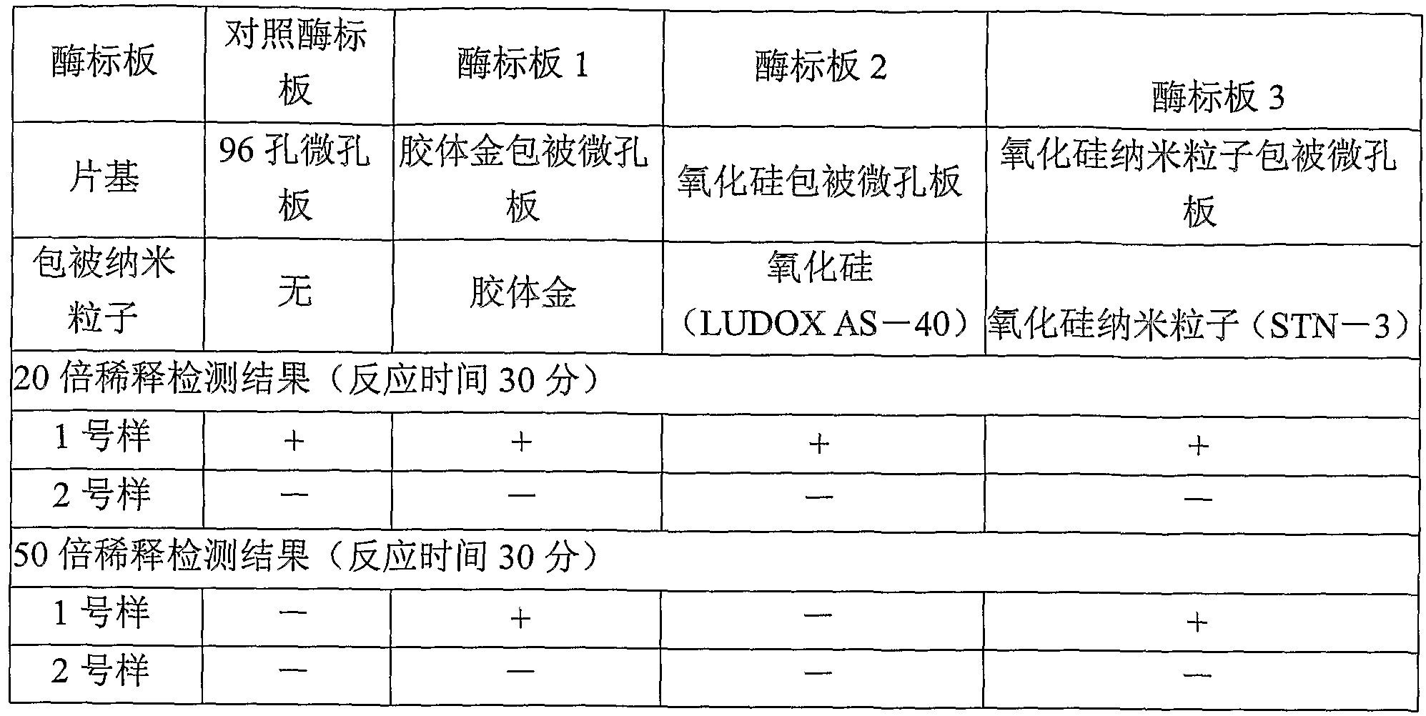

Claims
Priority Applications (4)
| Application Number | Priority Date | Filing Date | Title |
|---|---|---|---|
| CNB2004800006534A CN100410664C (en) | 2003-04-30 | 2004-04-30 | Device of containing Nano structure for analysis or separation, preparation method and application |
| EP04730459A EP1624306A4 (en) | 2003-04-30 | 2004-04-30 | Apparatus including nanostructures used for separation or analysis, and the preparation and application thereof |
| JP2006529552A JP2007502998A (en) | 2003-04-30 | 2004-04-30 | Apparatus for analyzing or separating nanometer structures, and its fabrication method and application |
| US11/258,996 US7842515B2 (en) | 2003-04-30 | 2005-10-27 | Nano-structured device for analysis or separation, and its preparation and application |
Applications Claiming Priority (6)
| Application Number | Priority Date | Filing Date | Title |
|---|---|---|---|
| CN03117787.5 | 2003-04-30 | ||
| CNA031177875A CN1514243A (en) | 2003-04-30 | 2003-04-30 | Method of preceeding qualitative and lor quantitative analysis against target substance its device and marker and detecting reagent box |
| CNPCT/CN04/00077 | 2004-01-20 | ||
| PCT/CN2004/000077 WO2004081571A1 (en) | 2003-03-13 | 2004-01-20 | The detecting method and device of polypeptide, and the ligand compound comprising nanoparticles |
| CNPCT/CN04/00203 | 2004-03-15 | ||
| PCT/CN2004/000203 WO2004090548A1 (en) | 2003-03-13 | 2004-03-15 | Device for analysis or separation containing an active nanostructured carrier, its preparation method and applications |
Related Parent Applications (1)
| Application Number | Title | Priority Date | Filing Date |
|---|---|---|---|
| PCT/CN2004/000077 Continuation WO2004081571A1 (en) | 2003-03-13 | 2004-01-20 | The detecting method and device of polypeptide, and the ligand compound comprising nanoparticles |
Related Child Applications (1)
| Application Number | Title | Priority Date | Filing Date |
|---|---|---|---|
| US11/258,996 Continuation US7842515B2 (en) | 2003-04-30 | 2005-10-27 | Nano-structured device for analysis or separation, and its preparation and application |
Publications (1)
| Publication Number | Publication Date |
|---|---|
| WO2004102196A1 true WO2004102196A1 (en) | 2004-11-25 |
Family
ID=33457894
Family Applications (1)
| Application Number | Title | Priority Date | Filing Date |
|---|---|---|---|
| PCT/CN2004/000437 WO2004102196A1 (en) | 2003-04-30 | 2004-04-30 | Apparatus including nanostructures used for separation or analysis, and the preparation and application thereof |
Country Status (2)
| Country | Link |
|---|---|
| EP (1) | EP1624306A4 (en) |
| WO (1) | WO2004102196A1 (en) |
Cited By (4)
| Publication number | Priority date | Publication date | Assignee | Title |
|---|---|---|---|---|
| WO2007015105A2 (en) * | 2005-08-04 | 2007-02-08 | Thomas William Rademacher | Nanoparticles comprising antibacterial ligands |
| WO2007085156A1 (en) * | 2006-01-25 | 2007-08-02 | Chengdu Kuachang Medical Industrial Limited | Active component, nanostructured composition comprising active components and its preparation |
| WO2007115444A1 (en) * | 2006-03-31 | 2007-10-18 | Chengdu Kuachang Medical Industrial Limited | Seperation or analysis composition comprising active nanostructure and seperation or analysis method |
| CN101443661B (en) * | 2006-01-25 | 2012-11-14 | 成都夸常医学工业有限公司 | Active constituent, nanostructure composition containing the active constituent and preparation method thereof |
Citations (21)
| Publication number | Priority date | Publication date | Assignee | Title |
|---|---|---|---|---|
| US5556756A (en) * | 1988-01-13 | 1996-09-17 | Nycomed As | Gold sol of less than 5 nm test method and reagent kit therefor |
| US5922537A (en) * | 1996-11-08 | 1999-07-13 | N.o slashed.AB Immunoassay, Inc. | Nanoparticles biosensor |
| US6154772A (en) * | 1997-11-04 | 2000-11-28 | Georgia Tech Research Corporation | System and method for the delivery of digital video and data over a communication channel |
| WO2000078362A2 (en) * | 1999-06-22 | 2000-12-28 | Aventis Research & Technologies Gmbh & Co. Kg | Stable, radioactively marked nanoparticles, method for the production and utilization thereof |
| CN1278534A (en) * | 2000-06-13 | 2001-01-03 | 复旦大学 | Polymer microball with fluorescent mark and its preparation |
| WO2001006257A1 (en) * | 1999-07-16 | 2001-01-25 | Wm. Marsh Rice University | Metal nanoshells for biosensing applications |
| CN1061372C (en) * | 1997-10-10 | 2001-01-31 | 中国科学院感光化学研究所 | Oxidase function compound sensitive film containing hydrophobic nanometre prill and its making method and use |
| US6268222B1 (en) * | 1998-01-22 | 2001-07-31 | Luminex Corporation | Microparticles attached to nanoparticles labeled with flourescent dye |
| WO2002006790A1 (en) * | 2000-07-14 | 2002-01-24 | Immunivest Corporation | Increased separation efficiency via controlled aggregation of magnetic nanoparticles |
| US6365362B1 (en) * | 1998-02-12 | 2002-04-02 | Immunivest Corporation | Methods and reagents for the rapid and efficient isolation of circulating cancer cells |
| CN1355319A (en) * | 2001-12-07 | 2002-06-26 | 清华大学 | Process for separating nucleic acid from biological particles by solid-phase carrier |
| CN1378083A (en) * | 2001-03-30 | 2002-11-06 | 清华大学 | Rare earth nano particle for biological material label and its preparing method and use |
| WO2002100805A2 (en) * | 2001-06-13 | 2002-12-19 | University Of Rochester | Colorimetric nanocrystal sensors, methods of making, and use thereof |
| US20020192654A1 (en) * | 2001-06-15 | 2002-12-19 | Tao-Kuang Chang | Bio-chip substrate for the embedding of DNA or protein and its fabrication method |
| CN1389539A (en) * | 2002-06-18 | 2003-01-08 | 高明远 | Prepn. and application of nano particle, nano microballoon and biological fuorescent probe |
| CN1390955A (en) * | 2002-07-26 | 2003-01-15 | 中国人民解放军第三军医大学 | Nano-class amplifying detection method for biochip |
| US20030013096A1 (en) * | 2000-03-16 | 2003-01-16 | Ichiro Yamashita | Nucleotide detector, process for producing the same and process for morming forming fine particle membrane |
| WO2003005029A2 (en) * | 2001-07-03 | 2003-01-16 | Governors Of The University Of Alberta | Magnetic nanoparticles for bioseparation application and methods for producing same |
| WO2003023402A1 (en) * | 2001-09-12 | 2003-03-20 | Sven Oscarsson | Immobilisation method and surfaces produced using said method |
| WO2003056336A2 (en) * | 2001-12-28 | 2003-07-10 | Fraunhofer-Gesellschaft zur Förderung der angewandten Forschung e.V. | Improved structured-functional bonding matrices for biomolecules |
| CN1456678A (en) * | 2002-05-09 | 2003-11-19 | 中南大学 | Biomarker-fluorescent silicon nano-particle preparing method |
Family Cites Families (2)
| Publication number | Priority date | Publication date | Assignee | Title |
|---|---|---|---|---|
| EP1135682B1 (en) * | 1998-11-30 | 2007-07-11 | Nanosphere, Inc. | Nanoparticles with polymer shells |
| US6689338B2 (en) * | 2000-06-01 | 2004-02-10 | The Board Of Regents For Oklahoma State University | Bioconjugates of nanoparticles as radiopharmaceuticals |
-
2004
- 2004-04-30 WO PCT/CN2004/000437 patent/WO2004102196A1/en active Application Filing
- 2004-04-30 EP EP04730459A patent/EP1624306A4/en not_active Ceased
Patent Citations (21)
| Publication number | Priority date | Publication date | Assignee | Title |
|---|---|---|---|---|
| US5556756A (en) * | 1988-01-13 | 1996-09-17 | Nycomed As | Gold sol of less than 5 nm test method and reagent kit therefor |
| US5922537A (en) * | 1996-11-08 | 1999-07-13 | N.o slashed.AB Immunoassay, Inc. | Nanoparticles biosensor |
| CN1061372C (en) * | 1997-10-10 | 2001-01-31 | 中国科学院感光化学研究所 | Oxidase function compound sensitive film containing hydrophobic nanometre prill and its making method and use |
| US6154772A (en) * | 1997-11-04 | 2000-11-28 | Georgia Tech Research Corporation | System and method for the delivery of digital video and data over a communication channel |
| US6268222B1 (en) * | 1998-01-22 | 2001-07-31 | Luminex Corporation | Microparticles attached to nanoparticles labeled with flourescent dye |
| US6365362B1 (en) * | 1998-02-12 | 2002-04-02 | Immunivest Corporation | Methods and reagents for the rapid and efficient isolation of circulating cancer cells |
| WO2000078362A2 (en) * | 1999-06-22 | 2000-12-28 | Aventis Research & Technologies Gmbh & Co. Kg | Stable, radioactively marked nanoparticles, method for the production and utilization thereof |
| WO2001006257A1 (en) * | 1999-07-16 | 2001-01-25 | Wm. Marsh Rice University | Metal nanoshells for biosensing applications |
| US20030013096A1 (en) * | 2000-03-16 | 2003-01-16 | Ichiro Yamashita | Nucleotide detector, process for producing the same and process for morming forming fine particle membrane |
| CN1278534A (en) * | 2000-06-13 | 2001-01-03 | 复旦大学 | Polymer microball with fluorescent mark and its preparation |
| WO2002006790A1 (en) * | 2000-07-14 | 2002-01-24 | Immunivest Corporation | Increased separation efficiency via controlled aggregation of magnetic nanoparticles |
| CN1378083A (en) * | 2001-03-30 | 2002-11-06 | 清华大学 | Rare earth nano particle for biological material label and its preparing method and use |
| WO2002100805A2 (en) * | 2001-06-13 | 2002-12-19 | University Of Rochester | Colorimetric nanocrystal sensors, methods of making, and use thereof |
| US20020192654A1 (en) * | 2001-06-15 | 2002-12-19 | Tao-Kuang Chang | Bio-chip substrate for the embedding of DNA or protein and its fabrication method |
| WO2003005029A2 (en) * | 2001-07-03 | 2003-01-16 | Governors Of The University Of Alberta | Magnetic nanoparticles for bioseparation application and methods for producing same |
| WO2003023402A1 (en) * | 2001-09-12 | 2003-03-20 | Sven Oscarsson | Immobilisation method and surfaces produced using said method |
| CN1355319A (en) * | 2001-12-07 | 2002-06-26 | 清华大学 | Process for separating nucleic acid from biological particles by solid-phase carrier |
| WO2003056336A2 (en) * | 2001-12-28 | 2003-07-10 | Fraunhofer-Gesellschaft zur Förderung der angewandten Forschung e.V. | Improved structured-functional bonding matrices for biomolecules |
| CN1456678A (en) * | 2002-05-09 | 2003-11-19 | 中南大学 | Biomarker-fluorescent silicon nano-particle preparing method |
| CN1389539A (en) * | 2002-06-18 | 2003-01-08 | 高明远 | Prepn. and application of nano particle, nano microballoon and biological fuorescent probe |
| CN1390955A (en) * | 2002-07-26 | 2003-01-15 | 中国人民解放军第三军医大学 | Nano-class amplifying detection method for biochip |
Non-Patent Citations (1)
| Title |
|---|
| See also references of EP1624306A4 * |
Cited By (5)
| Publication number | Priority date | Publication date | Assignee | Title |
|---|---|---|---|---|
| WO2007015105A2 (en) * | 2005-08-04 | 2007-02-08 | Thomas William Rademacher | Nanoparticles comprising antibacterial ligands |
| WO2007015105A3 (en) * | 2005-08-04 | 2007-11-01 | Thomas William Rademacher | Nanoparticles comprising antibacterial ligands |
| WO2007085156A1 (en) * | 2006-01-25 | 2007-08-02 | Chengdu Kuachang Medical Industrial Limited | Active component, nanostructured composition comprising active components and its preparation |
| CN101443661B (en) * | 2006-01-25 | 2012-11-14 | 成都夸常医学工业有限公司 | Active constituent, nanostructure composition containing the active constituent and preparation method thereof |
| WO2007115444A1 (en) * | 2006-03-31 | 2007-10-18 | Chengdu Kuachang Medical Industrial Limited | Seperation or analysis composition comprising active nanostructure and seperation or analysis method |
Also Published As
| Publication number | Publication date |
|---|---|
| EP1624306A1 (en) | 2006-02-08 |
| EP1624306A4 (en) | 2008-12-24 |
Similar Documents
| Publication | Publication Date | Title |
|---|---|---|
| US7842515B2 (en) | Nano-structured device for analysis or separation, and its preparation and application | |
| JP2007502998A5 (en) | ||
| US10191045B2 (en) | Sol composition for sol-gel biochip to immobilize probe on substrate without surface treatment and method and screening thereof | |
| JP3525142B2 (en) | Fluorescence analysis element using metal nanowell and method for producing the same | |
| JP2005524849A (en) | Nanoparticle probes for analyte detection with fingerprints for Raman spectroscopy | |
| Zubtsov et al. | Comparison of surface and hydrogel-based protein microchips | |
| JP2006330000A (en) | Improved biochip | |
| CA2428428A1 (en) | Protein chips, method producing it and detection system of the protein chips, and operating method of the detection system | |
| CN107298426B (en) | Magnetic microchip, preparation method and application with encoding of graphs | |
| Liu et al. | Advanced immobilization and amplification for high performance protein chips | |
| WO2004102196A1 (en) | Apparatus including nanostructures used for separation or analysis, and the preparation and application thereof | |
| US20060182655A1 (en) | Integrating analysis chip with minimized reactors and its application | |
| WO2007115444A1 (en) | Seperation or analysis composition comprising active nanostructure and seperation or analysis method | |
| KR100731913B1 (en) | Method for manufacturing nanohybrid particle using for biomolecule detection, biomolecule detection system, biomolecule detection method, and analysis apparatus using for biomolecule detection using nanohybrid particle | |
| US20030003480A1 (en) | Reactive solid support and DNA fragment detection tool | |
| JP4230126B2 (en) | Biological material chip | |
| WO2004081571A1 (en) | The detecting method and device of polypeptide, and the ligand compound comprising nanoparticles | |
| CN101013128A (en) | Analysis or separation facility containing nano structure | |
| WO2004090548A1 (en) | Device for analysis or separation containing an active nanostructured carrier, its preparation method and applications | |
| CA2100683A1 (en) | Scanning probe microscopy immunoassay | |
| Wang et al. | Microarray-Based Study of Carbohydrate–Protein Binding | |
| KR20080023278A (en) | Detecting method of dna hybridization using scattering | |
| JP2004177348A (en) | Method for detecting nucleic acid or protein with ultra-high sensitivity, detecting agent, and detection apparatus | |
| CN1987454B (en) | Nano structure component containing oriented nano structure functional zone and its preparing and applying method | |
| CN101443661B (en) | Active constituent, nanostructure composition containing the active constituent and preparation method thereof |
Legal Events
| Date | Code | Title | Description |
|---|---|---|---|
| AK | Designated states |
Kind code of ref document: A1 Designated state(s): AE AG AL AM AT AU AZ BA BB BG BR BW BY BZ CA CH CN CO CR CU CZ DE DK DM DZ EC EE EG ES FI GB GD GE GH GM HR HU ID IL IN IS JP KE KG KP KR KZ LC LK LR LS LT LU LV MA MD MG MK MN MW MX MZ NA NI NO NZ OM PG PH PL PT RO RU SC SD SE SG SK SL SY TJ TM TN TR TT TZ UA UG US UZ VC VN YU ZA ZM ZW |
|
| AL | Designated countries for regional patents |
Kind code of ref document: A1 Designated state(s): BW GH GM KE LS MW MZ NA SD SL SZ TZ UG ZM ZW AM AZ BY KG KZ MD RU TJ TM AT BE BG CH CY CZ DE DK EE ES FI FR GB GR HU IE IT LU MC NL PL PT RO SE SI SK TR BF BJ CF CG CI CM GA GN GQ GW ML MR NE SN TD TG |
|
| 121 | Ep: the epo has been informed by wipo that ep was designated in this application | ||
| WWE | Wipo information: entry into national phase |
Ref document number: 20048006534 Country of ref document: CN |
|
| WWE | Wipo information: entry into national phase |
Ref document number: 11258996 Country of ref document: US |
|
| WWE | Wipo information: entry into national phase |
Ref document number: 2006529552 Country of ref document: JP |
|
| WWE | Wipo information: entry into national phase |
Ref document number: 2004730459 Country of ref document: EP |
|
| WWE | Wipo information: entry into national phase |
Ref document number: 5522/DELNP/2005 Country of ref document: IN |
|
| WWP | Wipo information: published in national office |
Ref document number: 2004730459 Country of ref document: EP |
|
| WWP | Wipo information: published in national office |
Ref document number: 11258996 Country of ref document: US |